Clock recovery circuit and data receiving circuit

a clock recovery and data processing technology, applied in the field of clock recovery circuits and data receiving circuits, can solve the problems of affecting the performance of the chip, the speed gap between the elements or circuit blocks of the chip becoming a major factor limiting the performance improvement of the computer as a whole, and the inability to improve the system performance further, so as to reduce the jitter dependence of feedback loop characteristics, improve the predictability of characteristics, and reduce the amplitude of the limit cycle signal

Inactive Publication Date: 2009-09-03
FUJITSU LTD
View PDF6 Cites 1 Cited by
  • Summary
  • Abstract
  • Description
  • Claims
  • Application Information

AI Technical Summary

Benefits of technology

[0012]An object of the present invention is to reduce the amplitude of the limit cycle signal and also reduce the jitter dependence of feedback loop characteristics to improve the predictability of the characteristics, while at the same time, minimizing the phase noise that is caused by the phase modulation for linearization affecting the internal clock. Another object of the present invention is to reduce the quantization noise of the clock by increasing the resolution of the phase control code generating circuit.
[0021]The variation generating circuit may generate a zigzag wave-like variation changing by increasing and decreasing a plurality of times within one period of the variation. The variation generating circuit may generate a variation over a wide phase range when in an unstable state, and may generate a variation over a narrow phase range when in a stable state. The variation generating circuit may generate a variation of large gain when in an unstable state, and may generate a variation of small gain when in a stable state. The variation generating circuit may generate a variation with increased per-step unit time when in an unstable state, and may generate a variation with reduced per-step unit time when in a stable state.

Problems solved by technology

The improvements in the performance of semiconductor memory devices, processors, and the like have come to the point where system performance cannot be improved further unless the speed of signal transmission between components or elements is increased.
Specifically, the speed gap between a storage device such as a SRAM or DRAM (memory) and a processor (i.e., between LSIs), for example, has been widening year by year, and in recent years, this speed gap has been becoming a bottleneck impeding performance improvement for a computer as a whole.
Furthermore, with increasing integration and increasing size of semiconductor chips, the speed of signal transmission between elements or circuit blocks within a chip is becoming a major factor limiting the performance of the chip.
Moreover, the speed of signal transmission between a peripheral device and the processor / chipset is also becoming a factor limiting the overall performance of the system.

Method used


Image

  • Clock recovery circuit and data receiving circuit
  • Clock recovery circuit and data receiving circuit
  • Clock recovery circuit and data receiving circuit

Examples


first embodiment

[0189]FIGS. 30A and 30B are block diagrams showing the data receiving circuit according to the second mode of the present invention, wherein the circuit is configured as a 4-way×2 type interleaving circuit using CDR.

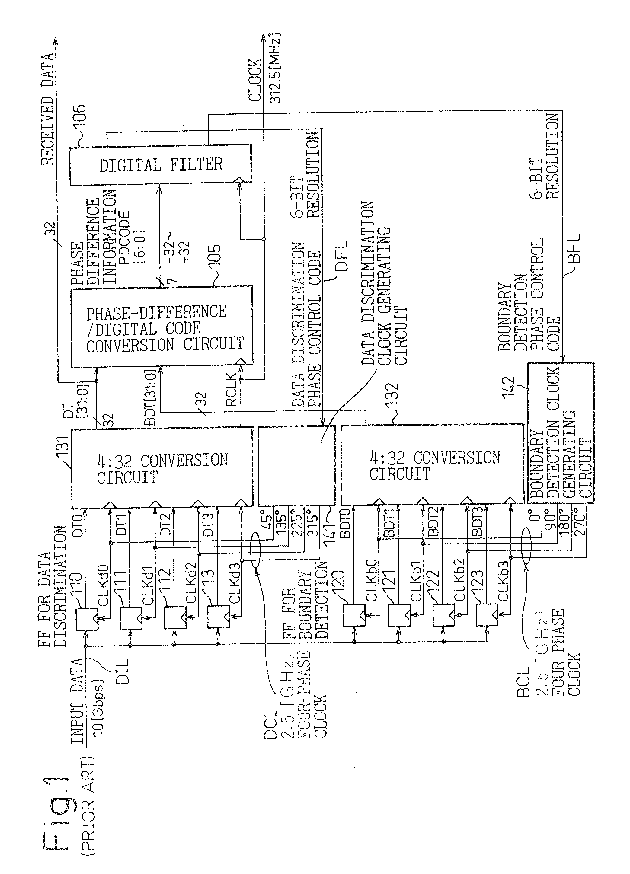
[0190]In FIGS. 30A and 30B, reference numerals 10 to 13 are data discrimination units (flip-flops for data discrimination, forming a data discrimination circuit), 20 to 23 are boundary detection units (flip-flops for boundary detection, forming a boundary detection circuit), 31 and 32 are data and boundary conversion circuits, respectively, 41 is a data discrimination clock generating circuit, 42 is a boundary detection clock generating circuit, 5 is a first phase-difference / digital-code conversion circuit, and 6 is a digital filter. Further, reference numeral 71 is a second phase-difference / digital-code conversion circuit, 72 is a first digital / analog converter (DAC), 73 is a second DAC, 74 is an adder, 75 is a voltage-controlled oscillator (VCO), and 76 is a buffer (cu...

second embodiment

[0218]FIGS. 38A and 38B are block diagrams showing the data receiving circuit according to the second mode of the present invention.

[0219]As is apparent from a comparison between FIGS. 38A, 38B and FIGS. 26A, 26B, the data receiving circuit of the second embodiment according to the second mode of the invention differs from the prior art configuration in that the digital filter 106 driven by the 312.5-MHz internal reference clock RCLK is replaced by two digital filters, i.e., the first digital filter 601 related to the first feedback loop (the low-frequency side feedback loop that provides the gain G1) and driven by a 312.5-MHz first internal reference clock RCLK-1, and the second digital filter 602 related to the second feedback loop (the high-frequency side feedback loop that provides the gain G2) and driven by a 625-MHz second internal reference clock RCLK-2.

[0220]The first digital filter 601 comprises a buffer 611 which provides gain G1 to the phase difference information PDCODE-...

third embodiment

[0232]FIGS. 42A and 42B are block diagrams showing the data receiving circuit according to the second mode of the present invention.

[0233]As is apparent from a comparison between FIGS. 42A, 42B and FIGS. 30A, 30B, 38A, and 38B, the data receiving circuit of the third embodiment according to the second mode of the invention is a combination of the data receiving circuit of the first embodiment according to the second mode of the invention and the data receiving circuit of the second embodiment according to the second mode. That is, as shown in FIGS. 42A and 42B, the data receiving circuit of the third embodiment according to the second mode of the invention is configured so that the output (here, PDCODE-2 [5:0]) of the second phase-difference / digital-code conversion circuit 71 in the data receiving circuit of the first embodiment shown in FIGS. 30A and 30B is supplied to the second digital filter 602 in the data receiving circuit of the second embodiment shown in FIGS. 38A and 38B. T...


PUM


Abstract

A clock recovery circuit has a boundary detection circuit detecting a boundary in an input signal in accordance with a first signal, and performs recovery of a clock by controlling the timing of the first signal in accordance with the detected boundary. The clock recovery circuit has a boundary detection timing varying circuit and a variation reducing circuit. The boundary detection timing varying circuit dynamically varies boundary detection timing in the boundary detection circuit by applying a variation to the first signal, and the variation reducing circuit reduces a phase variation occurring in the recovered clock in accordance with the dynamic variation of the boundary detection timing performed by the boundary detection timing varying circuit.

Description

CROSS REFERENCE TO RELATED APPLICATIONS[0001]This application is based upon and claims the benefit of priority from the prior Japanese Patent Application Nos. 2002-112347 filed on Apr. 15, 2002 and 2002-377931 filed on Dec. 26, 2002, the entire contents of which are incorporated herein by reference.BACKGROUND OF THE INVENTION[0002]1. Field of the Invention[0003]The present invention relates to a technology for enabling high-speed transmission of signals between a plurality of LSI chips or a plurality of devices or circuit blocks within a single chip, or between a plurality of boards or a plurality of cabinets and, more particularly, to a data receiving circuit and a clock recovery circuit that uses a feedback-loop-type clock signal generating circuit.[0004]2. Description of the Related Art[0005]Recently, the performance of components used in computers and other information processing apparatuses has been greatly improved. In particular, dramatic improvements have been made, for exam...

Claims


Application Information

Patent Timeline
Patent Type & Authority Applications(United States)
IPC IPC(8): H04L27/00G11C7/10H03L7/091H04L7/033
CPCG11C7/1078G11C7/1087H04L7/0331H03L7/091G11C7/222
Inventor YAMAGUCHI, HISAKATSUTAMURA, HIROTAKA
Owner FUJITSU LTD
Why Eureka
Try Eureka