Light emitting device of group iii nitride based semiconductor

a technology of nitride and light emitting device, which is applied in the direction of semiconductor devices, basic electric elements, electrical apparatus, etc., can solve the problems of reducing the total energy, increasing the difficulty of mass production, and variations in wavelength emitted, so as to achieve the effect of increasing optical efficiency

Inactive Publication Date: 2009-09-10
ADVANCED OPTOELECTRONICS TECH
View PDF10 Cites 44 Cited by
  • Summary
  • Abstract
  • Description
  • Claims
  • Application Information

AI Technical Summary

Benefits of technology

[0010]The primary aspect of the present invention is to provide a light emitting device of Group III nitride based semiconductor, which includes a stress relieving layer disposed between the quantum well layer and the barrier layer such that the lattice mismatch stress in the active layer can be relieved, and the optical efficiency can be increased.

Problems solved by technology

However, the structure is complex, and increases the difficulty of mass production.
However, this type of the structure will lower the total energy of the band gap of the active region 20 and results in variations of wavelength emitted.

Method used


Image

  • Light emitting device of group iii nitride based semiconductor
  • Light emitting device of group iii nitride based semiconductor
  • Light emitting device of group iii nitride based semiconductor

Examples


first embodiment

[0036]FIG. 5 is a schematic diagram of a light emitting diode device of Group III nitride based semiconductor according to the present invention. The light emitting diode device of Group III nitride based semiconductor 50 comprises a substrate 51, a buffer layer 52, an N-type semiconductor layer 53, an active layer 54, a current block layer 57 and a P-type semiconductor layer 58. The active layer 54 comprises at least one quantum well layer 56, a first barrier layer 541 and a second barrier layer 542. The first barrier layer 541 and the second barrier layer 542 are formed to sandwich the quantum well layer 56 therebetween. In addition, the active layer 54 further comprises a first stress relieving layer 551 and a second stress relieving layer 552. The first stress relieving layer 551 is disposed between the first barrier layer 541 and the quantum well layer 56, and the second stress relieving layer 552 is disposed between the second barrier layer 542 and the quantum well layer 56. T...

second embodiment

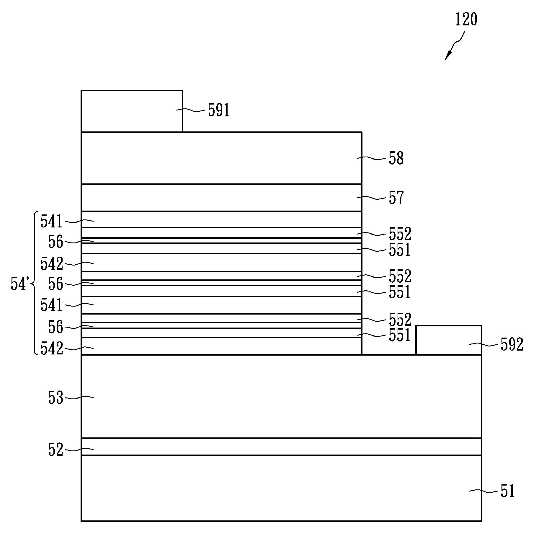
[0045]FIG. 12 is a schematic diagram of a light emitting device of Group III nitride based semiconductor according to the present invention. Compared to FIG. 5, the light emitting device of Group III nitride based semiconductor 120 has a structure including a plurality of quantum well layers. The active layer 54′ comprises three quantum well layers 56, and each quantum well layer 56 is sandwiched by a first stress relieving layer 551 and a second stress relieving layer 552. The first barrier layer 541 and the second barrier layer 542 are separately disposed outside of the first stress relieving layer 551 and the second stress relieving layer 552 such that the first stress relieving layer 551 and the second stress relieving layer 552 are sandwiched therebetween. The multiple quantum well layer structure can include different stacked layers of embodiments, for example, from 2 stacked layers to 30 stacked layers (in the present embodiment, the number of staked layers is 3). However, th...

third embodiment

[0048]FIG. 15 is a schematic diagram of a light emitting device of Group III nitride based semiconductor according to the present invention. The light emitting device of Group III nitride based semiconductor 150 comprises a substrate 51, a buffer layer 52, an N-type semiconductor layer 53, an active layer 54″, a current block layer 57, and a P-type semiconductor layer 58. The active layer 54″ comprises at least one quantum well layer 56 and the first barrier layer 541 and the second barrier layer 542 formed to sandwich the quantum well layer 56 therebetween. In addition, the active layer 54″, moreover, comprises a stress relieving layer 551′, and the stress relieving layer 551′ is disposed between the first barrier layer 541 and the quantum well layer 56, or is disposed between the second barrier layer 541 and the quantum well layer 56. The N-type semiconductor layer 53 further comprises an N-type electrode layer 592, and the P-type semiconductor layer 58 further comprises a P-type ...


PUM


Abstract

A light emitting device of Group III nitride based semiconductor comprises a substrate, an N-type semiconductor layer formed on the substrate, an active layer formed on the N-type semiconductor layer, and a P-type semiconductor layer formed on the quantum well layer. The active layer comprises at least one quantum well layer, at least two barrier layers formed to sandwich the quantum well layer therebetween and at least one stress relieving layer, wherein the stress relieving layer is interposed between the quantum well layer and one of the at least two barrier layers, and the composition of the stress relieving layer, made of Group III nitride based material, is graded along the direction from the quantum well layer to the barrier layers adjacent thereto.

Description

BACKGROUND OF THE INVENTION[0001]1. Field of the Invention[0002]The present invention relates to a light emitting device of Group III nitride based semiconductor, and relates more particularly to a light emitting device of Group III nitride based semiconductor, the active layer of which has increased lumen output and high optical efficiency.[0003]2. Description of the Related Art[0004]With wide application of light emitting diode (LED) devices in different products, semiconductor materials used for fabricating blue light LEDs are becoming the focus of much research in the optoelectronic industry. At present, semiconductor materials such as zinc selenide (ZnSe), silicon carbide (SiC), and indium gallium nitride (InGaN) are preferred for blue light LEDs, and these semiconductor materials have wide band gaps of above 2.6 eV. Because gallium nitride is a direct gap semiconductor, it can have high luminous flux, and compared to zinc selenide, which is also a direct gap semiconductor, the...

Claims


Application Information

Patent Timeline
Patent Type & Authority Applications(United States)
IPC IPC(8): H01L29/06H01L33/32
CPCH01L33/06H01L33/32H01L33/145
Inventor HUANG, SHIH CHENGYANG, SHUN KUEIHUANG, CHIA HUNGHSU, CHIH PENGCHAN, SHIH HSIUNG
Owner ADVANCED OPTOELECTRONICS TECH
Why Eureka
Try Eureka