

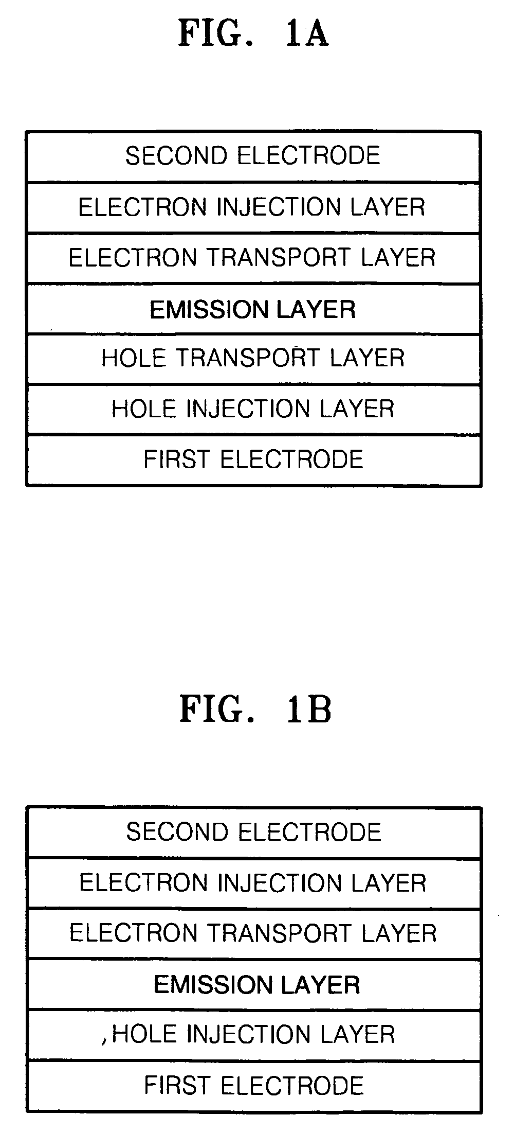
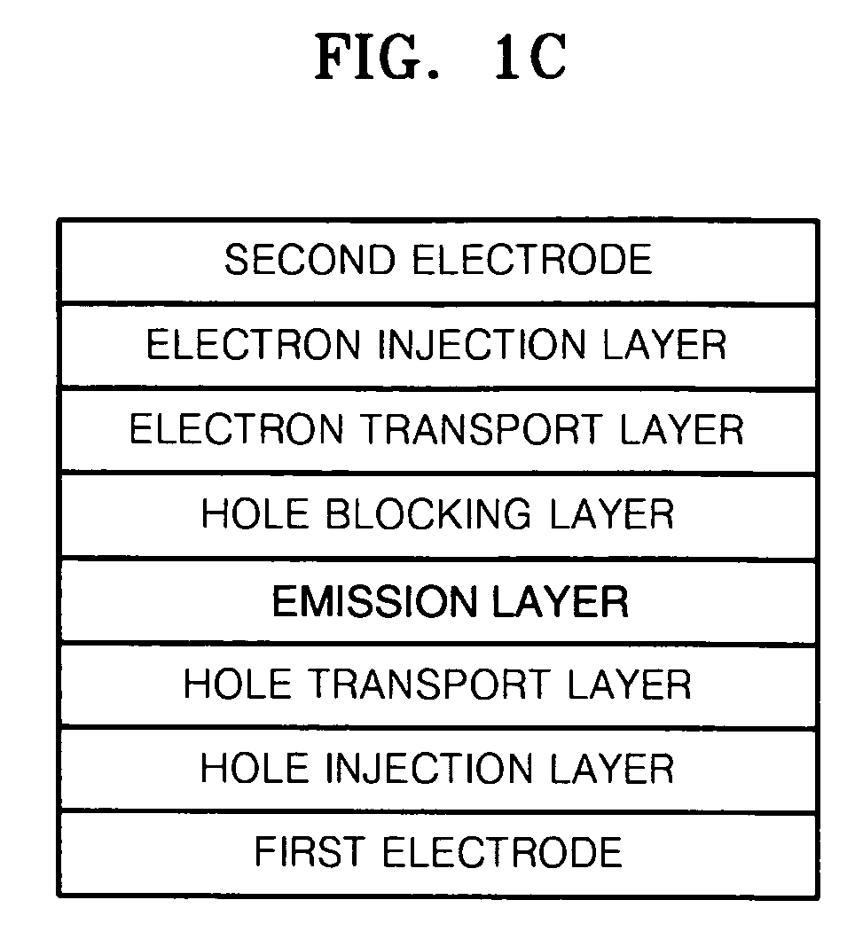
Indeno indene-based compound, organic light emitting device comprising the same, and method of manufacturing the organic light emitting device
- Summary
- Abstract
- Description
- Claims
- Application Information
AI Technical Summary
Benefits of technology
Problems solved by technology
Method used
Image

Examples
synthesis example 1
[0076]Compound 2 was Prepared.
[0077]Glass transition temperature (Tg), melting point (Tm), thermal degradation temperature (Td) and highest occupied molecular orbit (HOMO) of Compound 2 were measured. The results are shown in Table 1.
TABLE 1Compound No.Tg (° C.)Tm (° C.)Td (° C.)HOMO21282734185.87
[0078]Evaluation 1—Thermal Stability
[0079]The thermal stability of Compound 2 was measured based on Tg and Tm. Meanwhile, Tg and Tm of Comparative Compound A having the following structure (hereinafter referred to as “Compound A) were measured:
[0080]Tg and Tm were measured by performing a thermal analysis using thermo gravimetric analysis (TGA) and differential scanning calorimetry (DSC). The results are shown in Table 2:
TABLE 2Compound No.Tg (° C.)Tm (° C.)A129291
[0081]Therefore, it can be seen that a compound according to the present invention has a thermal stability suitable for use in an organic light emitting device.
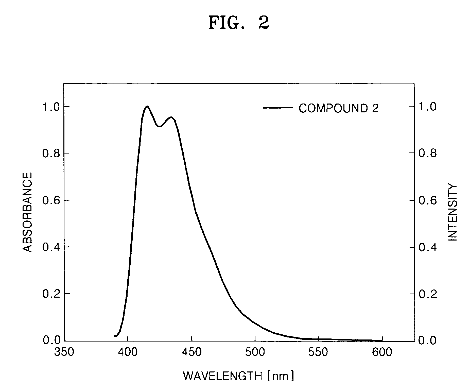
[0082]Evaluation 2: Emission Properties of Compound 2
[0083]Emission pr...
example 1
[0090]An organic light emitting device having the structure below was manufactured, wherein an emission layer was formed using a compound represented by Formula 8 acting as a dopant (hereinafter referred to as ‘dopant E605’) and Compound 2 acting as a host: ITO / PEDOT(500Å) / Compound 2_dopant E605(480Å) / Alq3(200Å) / LiF(10Å) / Al(2000Å).
[0091]A 15Ω / cm2 (1000Å) ITO glass substrate was cut to a size of 50 mm×50 mm×0.7 mm, and then sonicated with acetone isopropyl alcohol and pure water each for 15 minutes and washed with UV and ozone for 30 minutes, thereby forming an anode. Then, PEDOT-PSS (Al4083) manufactured by Bayer Co. was coated on the anode and then heat-treated at 110° C. for 5 minutes in air and heat-treated at 200° C. for 5 minutes in a nitrogen atmosphere, thereby forming a hole injection layer having a thickness of 500 Å. Then, a mixture including 1 g of Compound 2 acting as a host and 0.05 g of E605 was spin coated on the hole injection layer and then heat-treated at 110° C. f...
example 2
[0092]An organic light emitting device having the structure below was manufactured in the same manner as in Example 1, except that the emission layer was formed using only Compound 2: ITO / PEDOT(500Å) / Compound 2(480Å) / Alq3(200Å) / LiF(10 Å) / Al(2000Å). The obtained organic light emitting device will be referred to as Sample 2.
PUM
| Property | Measurement | Unit |
|---|---|---|
| Temperature | aaaaa | aaaaa |
| Temperature | aaaaa | aaaaa |
| Temperature | aaaaa | aaaaa |
Abstract
Description
Claims
Application Information