Deposition and Selective Removal of Conducting Helplayer for Nanostructure Processing

a technology of nanostructures and helplayers, applied in the field of chemical vapor deposition (cvd) of nanostructures, can solve the problems of affecting the compatibility of plasma gases and substrates or metal underlayers, arcs can damage the electronic devices connected damage to the growth structure, so as to avoid parasitic growth outside the catalyst, reduce the damage effect of sparks, and eliminate limitations on plasma gas compatibility

Active Publication Date: 2009-09-17
SMOLTEK AB
View PDF50 Cites 46 Cited by
  • Summary
  • Abstract
  • Description
  • Claims
  • Application Information

AI Technical Summary

Benefits of technology

[0031]Another advantage of the technology described herein is that sensitive electrical devices on the substrate are protected from the high voltages of the plasma, as all electrical connectors on the chip surface are shorted together and grounded. The technology described herein eliminates substantially all arcs, but even if there are some sparks (for example caused by static electricity during substrate handling) the damaging effect of the sparks is significantly reduced.
[0032]A third advantage is that the (possibly patterned) metal underlayer is protected from the plasma during the growth ...

Problems solved by technology

The problems will most often occur if there are insulating areas around the metal islands, even if the metal islands are electrically connected to other parts of the substrate.
Electric arcs will occur during the growth process, and cause damage to the growth structure due to sputtering.
The arcs can also damage the electronic devices connected to the growth structures by the over-voltages produced by the arcs. FIG. 2 shows an example of damage caused on a substrate due to arcing.
These over-voltages can damage the devices even if the devices are buried below several material layers, as the devices are electrically connected to the topmost metal layers.
U.S. Pat. No. 5,651,865 discloses using a periodic polarity change of the plasma voltage to preferentially sputter away any insulator from an otherwise conductive surface, which does not enable the nanostructure growth on samples with insulating regions.
With the methods disclosed in U.S. Pat. No. 6,982,519, it is not possible ...

Method used


Image

  • Deposition and Selective Removal of Conducting Helplayer for Nanostructure Processing
  • Deposition and Selective Removal of Conducting Helplayer for Nanostructure Processing
  • Deposition and Selective Removal of Conducting Helplayer for Nanostructure Processing

Examples


Embodiment Construction

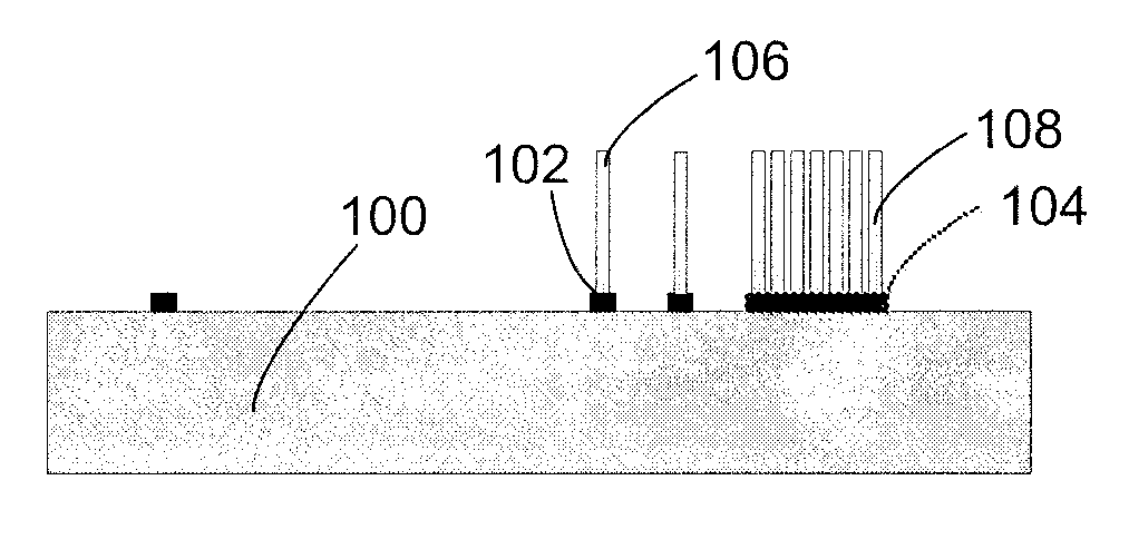
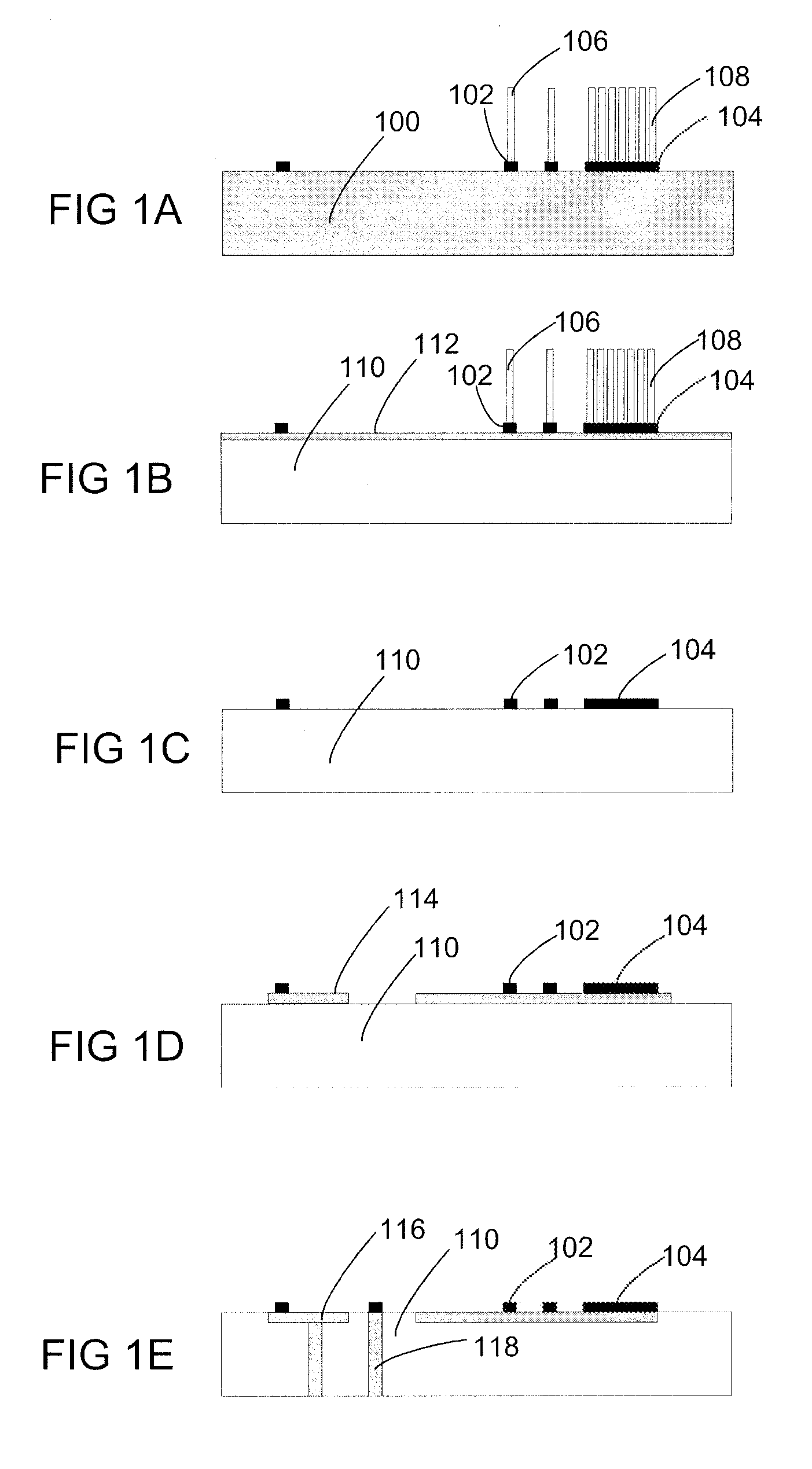
[0073]The technology described herein relates to plasma processing, for example, growth of nanostructures (i.e., structures having at least one dimension in the order of nanometers). In some implementations, the technology also applies to processing of structures with feature sizes other than in the nanometer range, for example in the micrometer or millimeter size range.

[0074]“Substrate” is a designation of any layer or layers on which other layers can be deposited for the growth of nanostructures. Substrates can include semiconductors containing devices or metal layers or insulators. Semiconductors can include doped or undoped silicon, silicon carbide, II-VI or III-V materials (GaAs, InP, InGaAs etc) or semiconducting polymers. A substrate can also be transparent, conducting or insulating materials such as glass or indium-tin-oxide (ITO). A substrate can also include polymer layers or printed circuit boards (PCBs). A substrate does not need to be flat and can contain corrugated str...


PUM

PropertyMeasurementUnit
Thicknessaaaaaaaaaa
Thicknessaaaaaaaaaa
Electrical conductoraaaaaaaaaa

Abstract

A method for making one or more nanostructures is disclosed, the method comprising: depositing a conducting layer on an upper surface of a substrate; depositing a patterned layer of catalyst on the conducting layer; growing the one or more nanostructures on the layer of catalyst; and selectively removing the conducting layer between and around the one or more nanostructures. A device is also disclosed, comprising a substrate, wherein the substrate comprises one or more exposed metal islands separated by one or more insulating areas; a conducting helplayer disposed on the substrate covering at least some of the one or more exposed metal islands or insulating areas; a catalyst layer disposed on the conducting helplayer; and one or more nanostructures disposed on the catalyst layer.

Description

CLAIM OF PRIORITY[0001]This application claims the benefit of priority of U.S. provisional application Ser. No. 61 / 031,333, filed on Feb. 25, 2008, the content of which is incorporated herein by reference in its entirety.TECHNICAL FIELD[0002]The technology described herein is generally related to the field of chemical vapor deposition (CVD) of nanostructures, and more specifically to reduction or elimination of plasma-induced damages during growth of nanostructures, and enabling self-aligned growth of nanostructures on both conducting and insulating surfaces.BACKGROUND[0003]The present technology described herein is related to but not limited to nanostructures such as carbon nanostructures (e.g., carbon nanotubes, carbon nanofibers, and carbon nanowires). These nanostructures have gained interest in recent years due to their high thermal and electrical conductivities.[0004]Carbon nanostructures can be manufactured with arc discharge methods, laser ablation, or chemical vapor deposit...

Claims


Application Information

Patent Timeline
IPC IPC(8): B32B15/00B05D5/12B44C1/22
CPCB82Y10/00B82Y40/00H01L2924/0002H01L21/0237H01L21/02491H01L21/02521H01L21/02603H01L21/02606H01L21/0262H01L21/02639H01L21/02645H01L21/76876H01L21/76879H01L29/0665H01L29/66439H01L2221/1094C01B31/0206H01L21/76877H01L23/49827H01L2924/00B82B3/00C23C16/44C01B32/15H01L21/3213H01B13/0026C23C16/26C23C16/503G02B6/26H01L21/4871H01L21/76802H01L23/3677H01L23/3737H01L23/5226H01L23/53276
Inventor BERG, JONAS S. T.DESMARIS, VINCENTKABIR, MOHAMMAD SHAFIQULSALEEM, MUHAMMAD AMINBRUD, DAVID
Owner SMOLTEK AB
Why Eureka
Try Eureka