Self-aligned field-effect transistor structure and manufacturing method thereof

a field-effect transistor and self-aligning technology, applied in the field of integrated circuit devices, can solve the problems of device field-effect characteristics loss, device hardly being able to constitute a fet, continuous decrease of the line width of the device, etc., and achieve the effect of simplifying the fabrication process

Inactive Publication Date: 2009-09-24
NATIONAL TSING HUA UNIVERSITY
View PDF8 Cites 15 Cited by
  • Summary
  • Abstract
  • Description
  • Claims
  • Application Information

AI Technical Summary

Benefits of technology

[0021]A carbon nanotube FET SEM fabricated according to an embodiment of the present invention and the field-effect characteristics thereof are shown in FIGS. 3 and 4. During the process of fabricating a carbon nanotube FET structure of the present invention, the carbon nanotube is directly formed between the catalytic source / drain containing CoSix for forming the carbon nanotube, thus omitting the step of additionally forming a catalyst layer of the carbon nanotube, so as to simplify the fabrication process. If the position of the source / drain of the FET is first defined through patterning, and then a carbon nanotube is formed by CVD, the purpose of mass production can be achieved.

Problems solved by technology

To follow the Moore's Law, the line width of a device is continuously decreased, and when a channel length drops to below 45 nm, the current MOSFET may face a technical bottleneck.
If the carbon nanotube 112 is metallic, the devices may lose the field-effect characteristics thereof and can hardly constitute an FET.
Moreover, the catalyst layer 108 may relatively complicate the mass production (as masks, pretreatment, process parameters, contact between the conductive source / drain and the catalyst layer should be considered).

Method used


Image

  • Self-aligned field-effect transistor structure and manufacturing method thereof
  • Self-aligned field-effect transistor structure and manufacturing method thereof
  • Self-aligned field-effect transistor structure and manufacturing method thereof

Examples


Embodiment Construction

[0028]Reference will now be made in detail to the present embodiments of the invention, examples of which are illustrated in the accompanying drawings. Wherever possible, the same reference numbers are used in the drawings and the description to refer to the same or like parts.

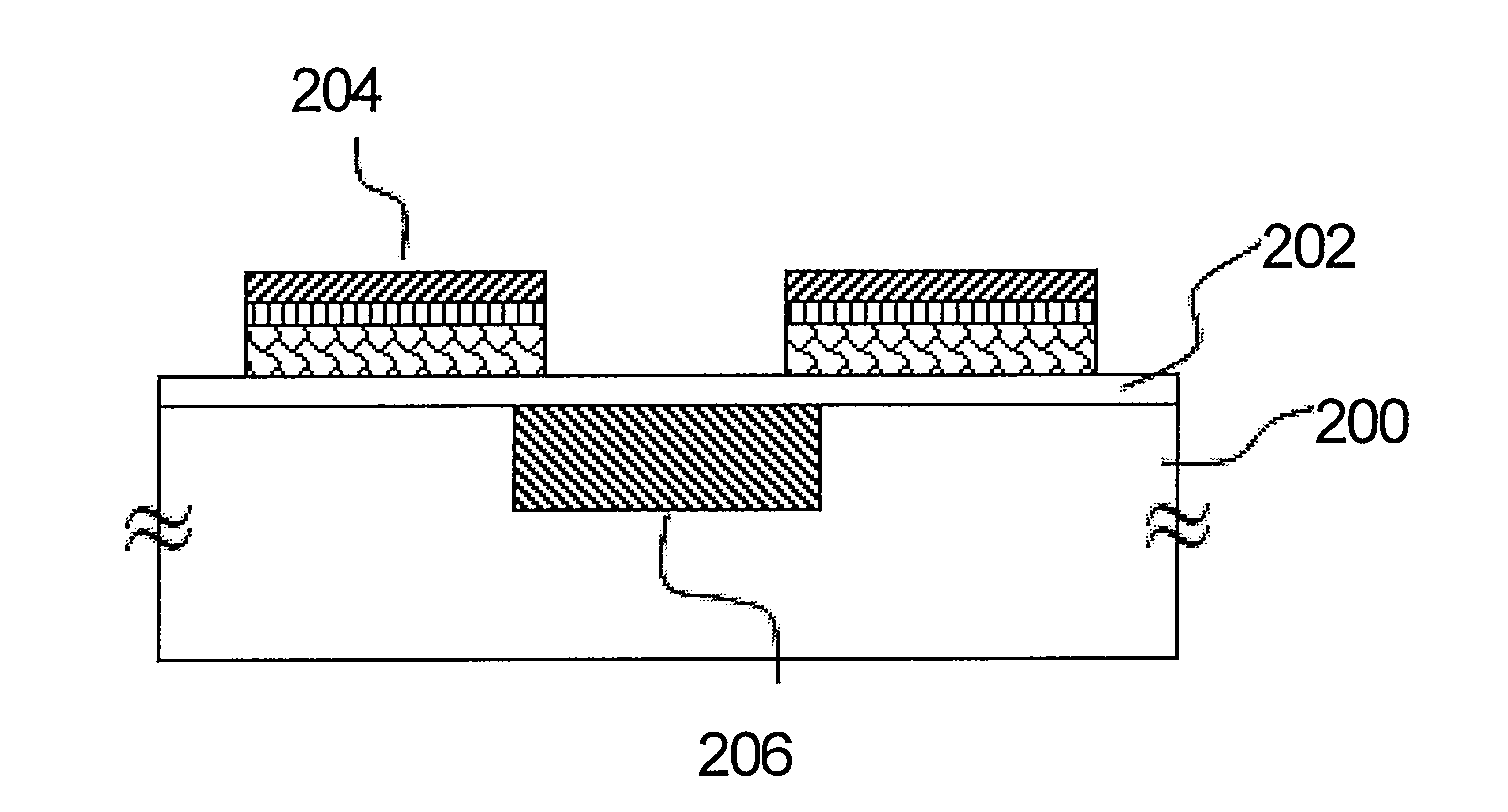
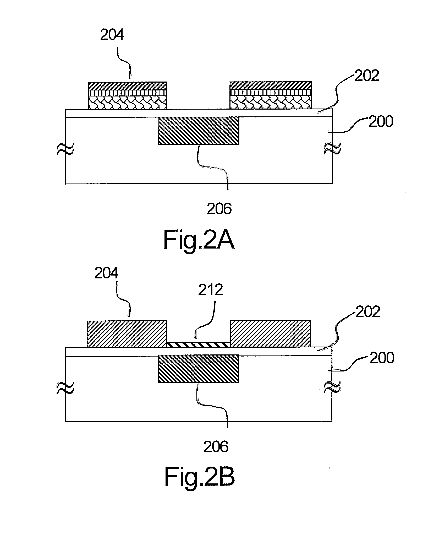
[0029]FIGS. 2A and 2B are cross-sectional views showing the process of fabricating a carbon nanotube FET structure according to an embodiment of the present invention. First, a substrate 200 having a gate 206 is provided. The gate 206 is made of, for example, a highly P-doped poly-Si by the following method. First, a highly doped poly-Si is deposited on the substrate 200, and then patterned to form the gate 206 through lithography and etching processes.

[0030]Next, referring to FIG. 2A, a dielectric layer 202 is formed on the gate 206. The dielectric layer 202 is made of, for example, SiO2, and the thickness of SiO2 ranges from 1 nm to 500 nm, preferably from 5 nm to 500 nm. Then, a catalytic source / drain 204 i...


PUM

PropertyMeasurementUnit
thicknessaaaaaaaaaa
thicknessaaaaaaaaaa
thicknessaaaaaaaaaa

Abstract

A self-aligned field-effect transistor (FET) is provided. The self-aligned FET includes a substrate, a dielectric layer, conductive electrodes, and a carbon nanotube. A patterned back-gated conductive electrode is disposed in the substrate. The dielectric layer is disposed on the substrate. The conductive electrodes are disposed on the dielectric layer and function as a source / drain. The patterned source / drain conductive electrodes contain a metal silicide such as cobalt silicide serve as a catalyst for carbon nanotube synthesis. The carbon nanotube is disposed on the dielectric layer to be electrically connected with the source / drain conductive electrodes.

Description

BACKGROUND OF THE INVENTION[0001]1. Field of the Invention[0002]The present invention generally relates to an integrated circuit device and a manufacturing method thereof, in particular, to a self-aligned field-effect transistor (FET) and a manufacturing method thereof.[0003]2. Description of Related Art[0004]For semiconductor devices of high integration, generally a metal-oxide-semiconductor field-effect transistor (MOSFET) is adopted as a basic logic device, and highly doped mono-Si and poly-Si are used to fabricate electrodes such as sources, drains, and gates. A dielectric layer is an oxide layer resulted from the oxidation of a silicon wafer at a high temperature. To follow the Moore's Law, the line width of a device is continuously decreased, and when a channel length drops to below 45 nm, the current MOSFET may face a technical bottleneck. Thereby, novel device design and material selection become critical.[0005]FIG. 1A is a schematic cross-sectional view of a conventional MO...

Claims


Application Information

Patent Timeline
Patent Type & Authority Applications(United States)
IPC IPC(8): H01L29/94H01L21/336
CPCB82Y10/00H01L51/0002H01L51/105H01L51/0545H01L51/0048H10K71/10H10K85/221H10K10/84H10K10/466
Inventor YANG, WEI-CHANGYEW, TRI-RUNG
Owner NATIONAL TSING HUA UNIVERSITY
Why Eureka
Try Eureka