Plasma etching apparatus and method, and computer-readable storage medium

a technology of etching apparatus and etching rate, which is applied in the direction of electrical apparatus, basic electric elements, electric discharge tubes, etc., can solve the problems of inability to completely solve the problem of hardware scale-up, inability to obtain plane etching uniformity, etc., to achieve the effect of simple and effective solution or correction, easy and efficient improvement of in-plane uniformity of etching rate, and easy and efficient improvement of characteristics or in-plane uniformity of etch

Inactive Publication Date: 2009-10-01
TOKYO ELECTRON LTD
View PDF5 Cites 41 Cited by
  • Summary
  • Abstract
  • Description
  • Claims
  • Application Information

AI Technical Summary

Benefits of technology

[0010]In view of the foregoing, the present invention provides a plasma etching apparatus capable of simply and effectively correcting or solving the problem of an unintended decrease of an etching rate of a central portion of the substrate lower than that of a periphery portion.
[0011]The present invention also provides a plasma etching apparatus capable of easily improving characteristics or in-plane uniformity of the etching of an organic film without the expense of deteriorating characteristics or in-plane uniformity of the etching of a non-organic film under the same hardware.
[0012]Further, the present invention also provides a plasma etching method capable of easily and efficiently improving in-plane uniformity of etching rate on a target substrate in the etching of an organic film, and also provides a computer readable storage medium to be used therein.

Problems solved by technology

As a result, in-plane etching uniformity cannot be obtained, and it is known that this problem cannot be completely resolved only by the above-described upper-side DC application method.
However, such approach not only causes a scale-up of hardware but also causes another (even worse) problem that the in-planed uniformity cannot be maintained because the etching rate of the substrate central portion becomes excessively higher than the etching rate of the substrate periphery portion when etching the processing target film.
Thus, this solution has no practical use.

Method used


Image

  • Plasma etching apparatus and method, and computer-readable storage medium
  • Plasma etching apparatus and method, and computer-readable storage medium
  • Plasma etching apparatus and method, and computer-readable storage medium

Examples


first embodiment

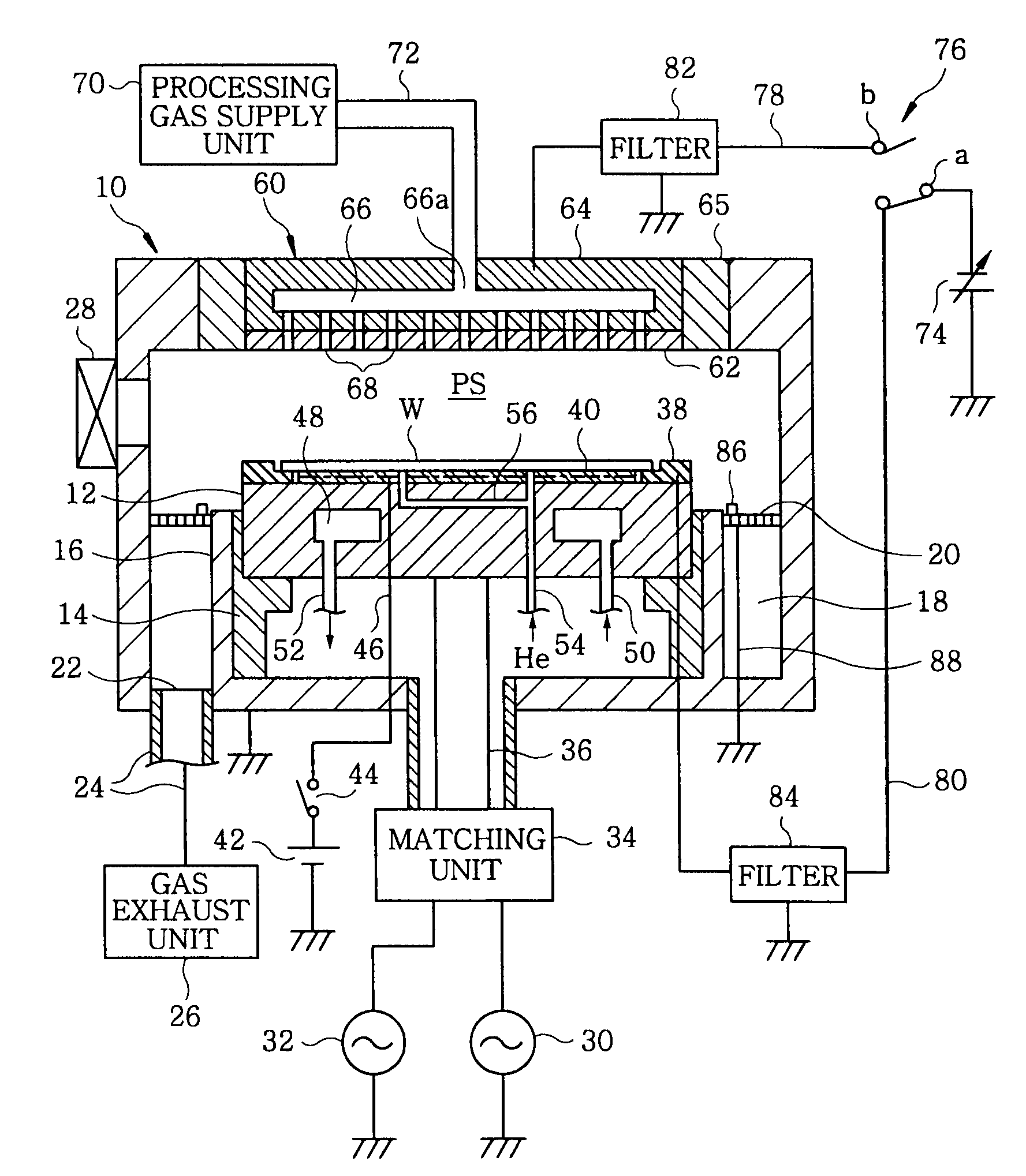
[0042]FIG. 1 illustrates a configuration of a plasma etching apparatus in accordance with the present invention. The plasma etching apparatus is configured as a capacitively coupled plasma etching apparatus of a cathode-coupled type employing a lower-side dual frequency application mechanism. The plasma etching apparatus includes a cylindrical chamber (processing vessel) 10 made of a metal such as aluminum, stainless steel, or the like. The chamber 10 is frame-grounded.

[0043]A circular plate-shaped susceptor 12 for mounting, for example, a semiconductor wafer W thereon is horizontally installed in the chamber 10 to be used as a lower electrode. The susceptor 12 is made of, for example, aluminum and is supported on an insulating cylindrical support 14 extended vertically upward from the bottom of the chamber 10. An annularly shaped gas exhaust path 18 is formed between a sidewall of the chamber 10 and a conductive cylindrical support (inner wall portion) 16 extended vertically upward...

second embodiment

[0086]The characteristic of the second embodiment pertains to a DC ground component (DC ground electrode) 86.

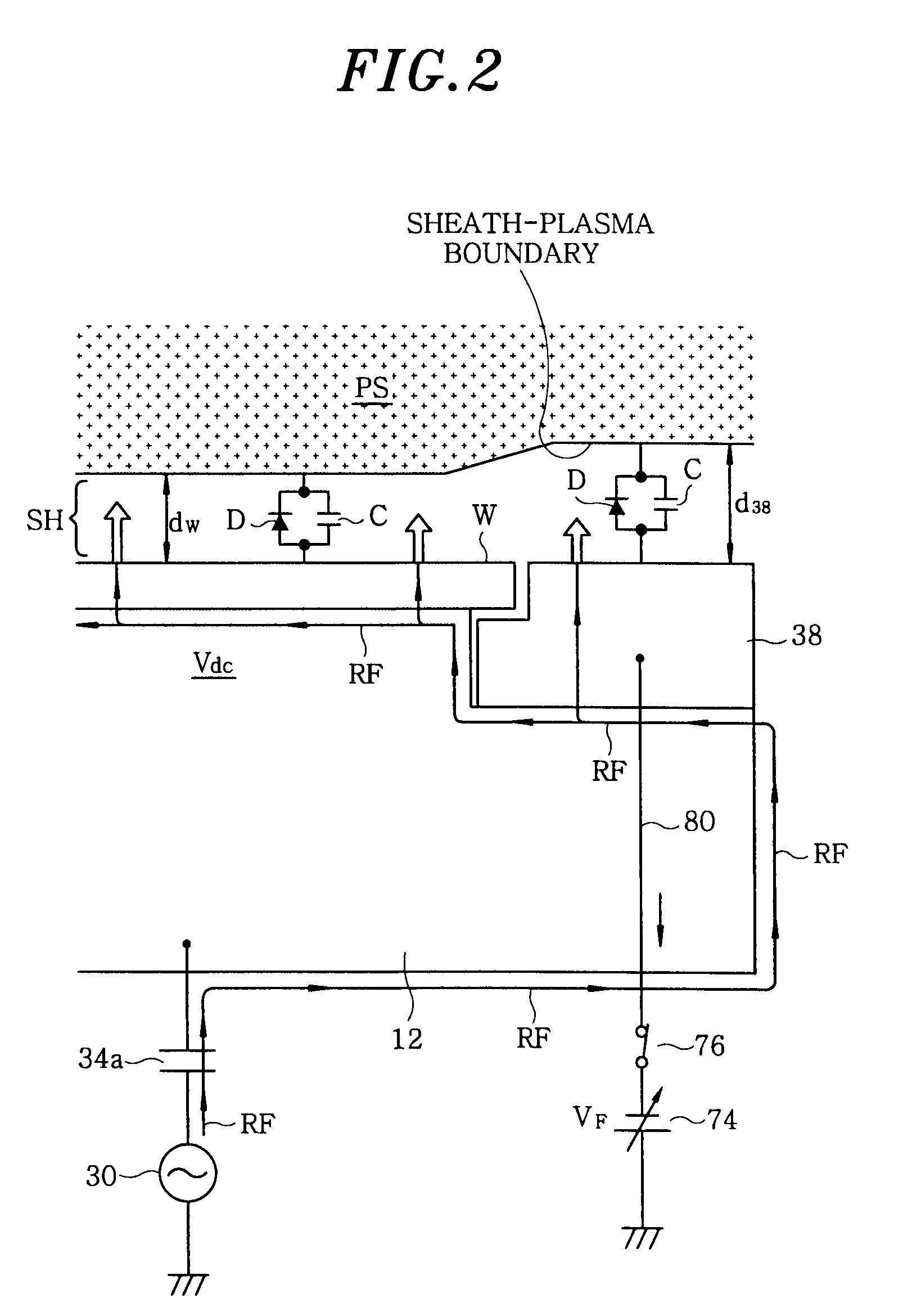
[0087]As described above, if the DC voltage is applied to the focus ring 38 and / or the upper electrode 60, electrons would be accumulated in these members, raising a likelihood that an abnormal discharge may be generated between these members and the chamber sidewall or the like. However, by providing the DC ground component 86 at a proper number of locations exposed to plasma, the electrons accumulated in the focus ring 38 or the upper electrode 60 would arrive at the DC ground component 86 through the plasma and would be discharged from there into a ground line through the chamber sidewall, so that the abnormal discharge can be prevented.

[0088]However, if deposits such as polymer generated during the etching process are adhered to the surface of the DC ground component 86, the DC grounding function would be deteriorated, and the effects of the focus-ring DC application meth...


PUM

PropertyMeasurementUnit
frequencyaaaaaaaaaa
frequencyaaaaaaaaaa
DC voltageaaaaaaaaaa

Abstract

A plasma etching apparatus includes a processing vessel; a lower electrode on which a target substrate is mounted in the processing vessel; an upper electrode disposed in the processing vessel to face the lower electrode in parallel; a processing gas supply unit configured to supply a processing gas into a processing space between the upper and the lower electrode; a first radio frequency power supply unit configured to apply, to the lower electrode, a first radio frequency power for generating plasma of the processing gas; a focus ring covering a top surface peripheral portion of the lower electrode protruding toward a radial outside of the substrate; a DC power supply configured to output a variable DC voltage; and a DC voltage supply network that connects the DC power supply to either one of the focus ring and the upper electrode or both depending on processing conditions of plasma etching.

Description

FIELD OF THE INVENTION[0001]The present invention relates to a capacitively coupled plasma etching apparatus for performing a dry etching process on a target substrate by using plasma; a plasma etching method; and a computer-readable storage medium.BACKGROUND OF THE INVENTION[0002]Etching, which is employed in a manufacturing process of a semiconductor device or a FPD (Flat Panel Display), is a technique for processing a film on the surface of a target substrate (a semiconductor wafer, a glass substrate, or the like) into a desired circuit pattern by using a resist pattern, which is formed by a lithography technique, as a mask. Conventionally, a capacitively coupled plasma etching apparatus has been a mainstream of single-wafer etching apparatuses.[0003]Generally, the capacitively coupled plasma etching apparatus has a configuration in which an upper electrode and a lower electrode are disposed in parallel to each other in a processing vessel configured as a vacuum chamber. In this ...

Claims


Application Information

Patent Timeline
Patent Type & Authority Applications(United States)
IPC IPC(8): H01L21/306
CPCH01J37/32091H01J37/32165H01L21/31138H01J37/32697H01J37/32642
Inventor KOSHIMIZU, CHISHIOIWATA, MANABUHONDA, MASANOBUNAKAYAMA, HIROYUKI
Owner TOKYO ELECTRON LTD
Why Eureka
Try Eureka