
Integrated Wideband RF Tracking Filter for RF Front End with Parallel Band Switched Tuned Amplifiers

a wideband, filter technology, applied in the field of radio frequency (rf) tuners, can solve the problems of low power consumption, long battery life, and power consumption in silicon rf tuners is the receiver architecture, and achieve the effect of uniform gain

Inactive Publication Date: 2009-10-08
NXP BV
View PDF21 Cites 54 Cited by
  • Summary
  • Abstract
  • Description
  • Claims
  • Application Information

AI Technical Summary

Benefits of technology

[0022]The RF filter and methods described above can be used in TV set-up boxes or digital TVs for terrestrial / cable and satellite broadcasts. It can be in general applied to any other broad band communication systems such as ultra wide band (UWB) and wireless high-definition television (wireless HD).

Problems solved by technology

However, for a wireless application low power consumption is extremely desirable as it leads to longer battery life.
Another dominant source of power consumption in silicon RF tuners is the receiver architecture.
However, super-heterodyne receivers consume a great deal of power due to its two frequency conversion stage architecture.
However, due to the proximity in frequency of the local oscillator signal to the input signal frequency a direct conversion receiver in broad band tuner applications is susceptible to undesired adjacent and alternate channels at the frequency of LO harmonics.
This would result an undesired effect that any signals at 150 MHz and 250 MHz are downconverted to a baseband signal as well as the desired signal at 50 MHz.
The net result is that the interference from the LO harmonics can be quite significant and can desensitize the receiver.
One of the major reasons for the high linearity requirements is because non-linearity in a receiver leads to inadvertent frequency mixing, that is signals residing in different channels can get mixed together some of which can result in interference in the desired channel.
As a result, since an RF tracking filter attenuates undesired channels over the enter frequency band.
Chief among the challenges are minimizing the chip area and the power consumption, in particular the amount of current required.
While suitable for some applications, these different topologies have significant drawbacks making them unsuitable for or at a minimum difficult to use in wide band receiver applications.
While this topology provides attenuation up to 50 dB, it suffers from a discrete implementation comprising components to bulky to be efficiently integrated into a silicon tuner.
Additionally, there is a loss of approximately 5 dB by using a purely passive component.
A loss introduced by the tracking filter results in a higher noise contribution from the following blocks of a receiver and therefore makes the overall noise figure of the tuner higher.
While this design resolves some of the deficiencies of previous designs, it still suffers from several weaknesses that make it impractical for integrate silicon broad band applications.
1445-1448) shows that the dynamic range is limited which results in a high noise figure and a low IP3, insufficient for wide band receiver applications.
In addition this design does not provide adequate tuning range for the wide band receiver applications.
Further, the presence of inductors in the form of transformers is too costly in terms of chip area.
However, the disclosure does not discuss any specific dynamic range performance or tuning bandwidth coverage for comparison with other topologies.
However, there are several drawbacks that prohibit use of the RF MEMs filters for cable, terrestrial, and satellite TV bands.
The first limitation is the center frequencies of the bands, which are much higher than the desired 50 to 850 MHz for TV applications.
Secondly, the filter requires an extremely large chip area of 32 mm2, which is nearly twice the size of most RF Silicon tuner chips used for these applications and would nearly triple the wafer costs.
Also, the filter requires very expensive wafer post processing steps beyond conventional SiGe BiCMOS or CMOS technologies to add the MEMS filter structures.
Lastly, the filter is passive and therefore not capable of providing any gain to limit the noise figure contribution of the back end receiver, making it impractical to be integrated into the RF front end of the tuner.

Method used


Image

  • Integrated Wideband RF Tracking Filter for RF Front End with Parallel Band Switched Tuned Amplifiers
  • Integrated Wideband RF Tracking Filter for RF Front End with Parallel Band Switched Tuned Amplifiers
  • Integrated Wideband RF Tracking Filter for RF Front End with Parallel Band Switched Tuned Amplifiers

Examples


Embodiment Construction

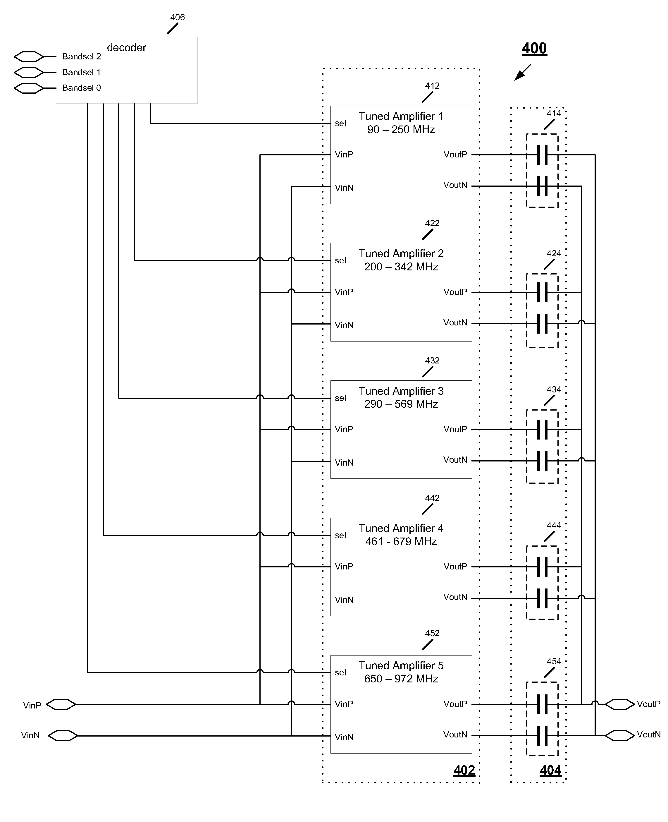
[0038]Embodiments of the present invention resolve many of the difficulties in implementing an RF tracking filter in an integrated broad band application. FIG. 4 illustrates an embodiment of an RF tracking filter for broad band applications. Filter 400 comprises a plurality of parallel tuned amplifiers 402. The plurality of parallel tuned amplifiers 402 are coupled to a common differential output through a plurality of pairs of coupling capacitors 404. More specifically, a differential input signal is supplied to each of the tuned amplifiers and coupled to a common differential output through a pair of coupling capacitor for each amplifier. For example, tuned amplifier 432 is coupled to the differential output through coupling capacitors 434. Each of the tuned amplifiers is designed to cover a different band within the overall frequency range. In order to account for the presents of mismatch and process-voltage-temperature (PVT) center frequency shift, the bands should overlap with ...


PUM


Abstract

A wideband RF tracking filter having a set of parallel tuned resonator amplifier stages with a de-Q resistor for each subband is disclosed. The resonant amplifier contains programmable tuned LC tank impedance and an array of parallel voltage to current converters (V2I) for each subband. The de-Q resistor together with the array of V2I converters provides a flat gain over each subband and each of the other subbands covering different frequencies.

Description

BACKGROUND OF THE INVENTION[0001]1. Field of the Inventions[0002]The present invention relates to radio frequency (RF) tuners and specifically to integrated RF tracking filters.[0003]2. Background Information[0004]Following the integration trend in silicon, broadband tuners have also been integrated onto a single silicon chip. Many new applications such as Digital Video Broadcast-Handheld (DVB-H), Universal Serial Bus (USB) TV tuners for the personal computer, and dual tuners for Digital Video Recorder (DVR) have placed a premium on reduction of power. For example, low power DVB-H tuners can enable TV tuners to be integrated into wireless applications. However, for a wireless application low power consumption is extremely desirable as it leads to longer battery life. Low power consumption is very desirable for applications such as USB TV tuners to fit within the power supply capabilities of the USB interface. Furthermore, lower power consumption means lower heat dissipation requirem...

Claims


Application Information

Patent Timeline
IPC IPC(8): H04L27/06H04N5/50H04N7/16
CPCH03J5/244
Inventor GAO, WEINANROSIK, RAY
Owner NXP BV
Learn More