Magnetoresistive element and magnetic random access memory

a magnetic random access and magnetic element technology, applied in the field of magnetoresistive elements and magnetic random access memory, can solve the problems of difficult to achieve both a low electric current and memory cell micropatterning

Inactive Publication Date: 2009-10-08
KK TOSHIBA
View PDF48 Cites 73 Cited by
  • Summary
  • Abstract
  • Description
  • Claims
  • Application Information

AI Technical Summary

Benefits of technology

[0011]A magnetoresistive element according to an aspect of the present invention comprises a foundation layer, a first magnetic layer on the foundation layer, a tunnel barrier layer on the first magnetic layer, and a second magnetic layer on the tunnel barrier layer. The magnetization direction in one of the first and second magnetic layers is invariable, and the magnetization direction in the other is...

Problems solved by technology

This makes it difficult to achieve both a low electric current and mem...

Method used


Image

  • Magnetoresistive element and magnetic random access memory
  • Magnetoresistive element and magnetic random access memory
  • Magnetoresistive element and magnetic random access memory

Examples


experimental example 1

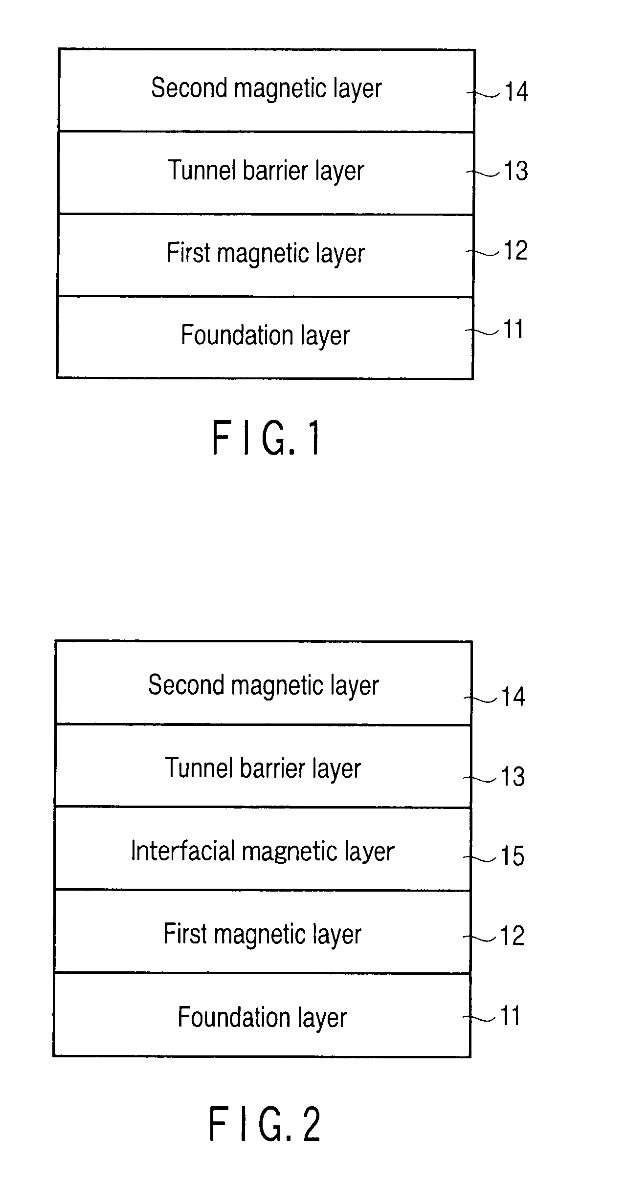
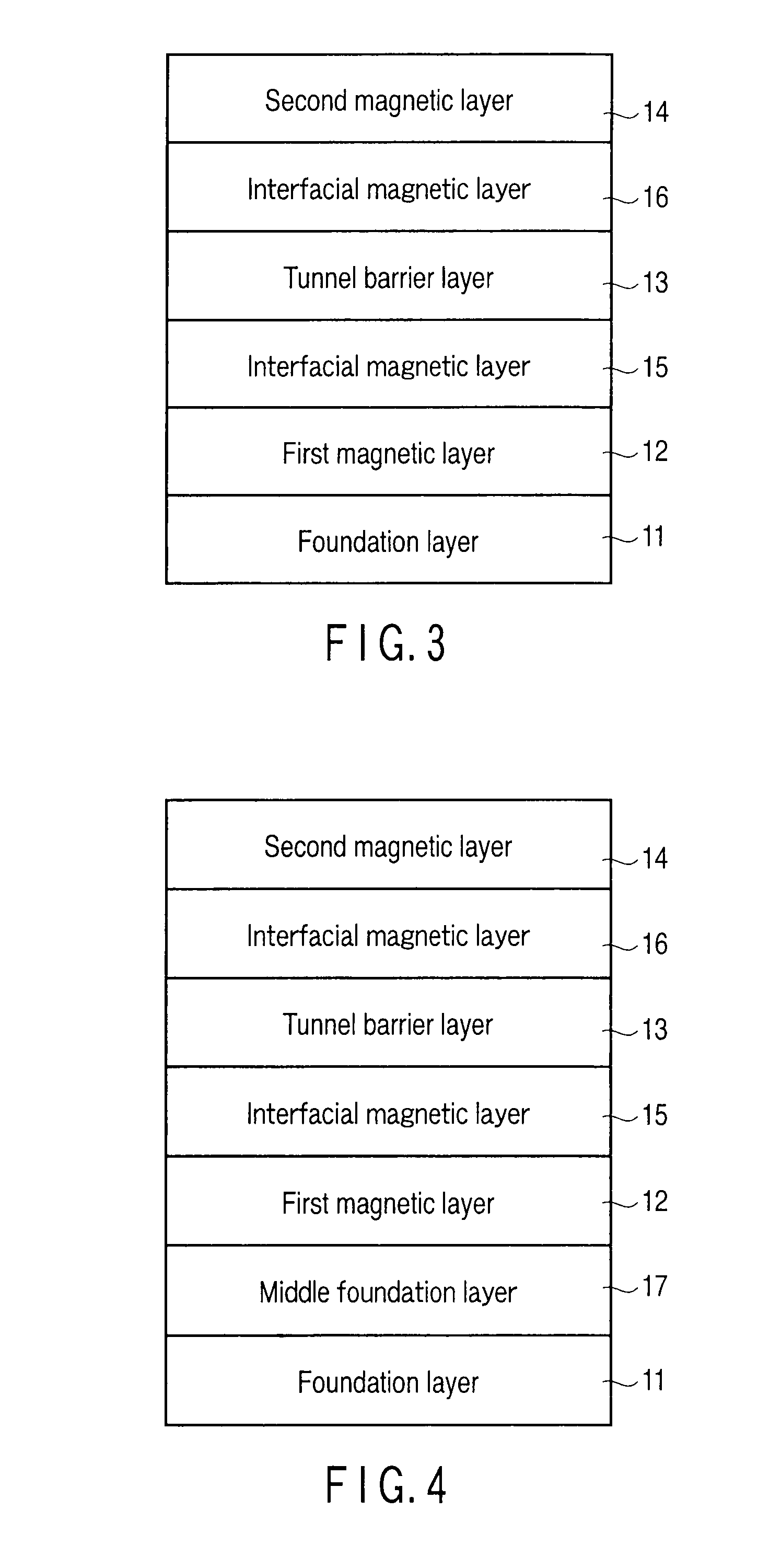
[0222]The magnetoresistive element had a cap layer / TbCoFe ferromagnetic layer (30 nm) / MgO tunnel barrier layer (1.5 nm) / CoFeB interfacial magnetic layer (1 nm) / L10-FePt ferromagnetic layer (5 nm) / Pt middle foundation layer (3 nm) / Fe foundation layer (10 nm) / Cr foundation layer (10 nm) / NiTa foundation layer (20 nm) / Ta foundation layer (5 nm) / thermal oxide Si layer (potential resetting layer) in this order from the upper layer side.

experimental example 2

[0223]The magnetoresistive element had a cap layer / L10-FePt ferromagnetic layer (3 nm) / MgO tunnel barrier layer (1.5 nm) / CoFeB interfacial magnetic layer (2 nm) / L10-FePt ferromagnetic layer (10 nm) / Pt middle foundation layer (3 nm) / Cr foundation layer (20 nm) / NiTa foundation layer (20 nm) / Ta foundation layer (5 nm) / thermal oxide Si layer (potential resetting layer) in this order from the upper layer side.

[0224]In each sample, the nitride resetting layer and thermal oxide Si layer functioned as potential resetting layers for preventing generation of the surface electric charge. Also, after each layer was formed, vacuum annealing was performed to optimize the TMR characteristics and magnetic characteristics.

[0225]Sectional TEM observation was performed on the three samples described above, thereby evaluating and examining the crystallinity of each MgO tunnel barrier layer.

[0226]In Comparative Example 1, the MgO tunnel barrier layer was found to be amorphous by X-ray diffraction becaus...

application examples

4. APPLICATION EXAMPLES

[0229]Application examples of the present invention will be explained below.

(1) Spin Injection Magnetic Random Access Memory

[0230]The magnetoresistive element according to the example of the present invention is particularly effective in a spin injection magnetic random access memory which has a write circuit for supplying a write current from one terminal to the other of the magnetoresistive element or vice versa, and in which the write current changes the relationship between the magnetization directions in first and second magnetic layers.

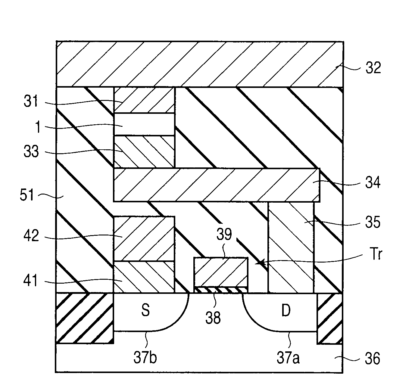
[0231]FIG. 9 shows a memory cell of the spin injection magnetic random access memory.

[0232]The upper end of a magnetoresistive element 1 is connected to an upper bit line 32 via an upper electrode 31. The lower end of the magnetoresistive element 1 is connected to a drain diffusion layer 37a of a select transistor Tr via a lower electrode 33, extraction electrode 34, and plug 35.

[0233]A source diffusion layer 37b of the se...


PUM


Abstract

A magnetoresistive element includes a foundation layer, a first magnetic layer on the foundation layer, a tunnel barrier layer on the first magnetic layer, and a second magnetic layer on the tunnel barrier layer. The first magnetic layer is made of a ferromagnetic metal containing one or more elements selected from a first group consisting of Co, Fe, and Ni, and one or more elements selected from a second group consisting of Cu, Ag, Au, Pd, Pt, Ru, Rh, Ir, and Os. The foundation layer is made of a metal containing one or more elements selected from a third group consisting of Al, Ni, Co, Fe, Mn, Cr, and V.

Description

CROSS-REFERENCE TO RELATED APPLICATIONS[0001]This application is based upon and claims the benefit of priority from prior Japanese Patent Application No. 2008-084939, filed Mar. 27, 2008, the entire contents of which are incorporated herein by reference.BACKGROUND OF THE INVENTION[0002]1. Field of the Invention[0003]The present invention relates to a magnetoresistive element and magnetic random access memory.[0004]2. Description of the Related Art[0005]Recently, many solid-state memories that record information on the basis of new principles have been proposed. A magnetoresistive random access memory (to be referred to as an MRAM hereinafter) using the tunneling magnetoresistive effect (to be also referred to as a TMR (Tunneling Magneto Resistance) hereinafter) is particularly known as a solid-state magnetic memory. The MRAM uses a magnetoresistive element (to be referred to as a TMR element hereinafter) having the magnetoresistive effect as a memory element of a memory cell. The me...

Claims


Application Information

Patent Timeline
IPC IPC(8): G11C11/00H01L29/82G11C11/416G11C11/14
CPCB82Y10/00B82Y25/00G11B5/3906G11B5/3909G11C11/16H01F10/123H01F41/307H01L27/228H01L43/08H01F10/3286H01F10/329H01F10/3254G11C11/161G11C11/1675H10B61/22H10N50/10
Inventor YOSHIKAWA, MASATOSHIKITAGAWA, EIJIDAIBOU, TADAOMINAGAMINE, MAKOTOKISHI, TATSUYAYODA, HIROAKI
Owner KK TOSHIBA
Why Eureka
Try Eureka