

Method of growing an active region in a semiconductor device using molecular beam epitaxy
a technology of molecular beam and active region, which is applied in the direction of lasers, nanoinformatics, semiconductor lasers, etc., can solve the problems of low device yield and poor sample uniformity
- Summary
- Abstract
- Description
- Claims
- Application Information
AI Technical Summary
Problems solved by technology
Method used
Image

Examples
first embodiment
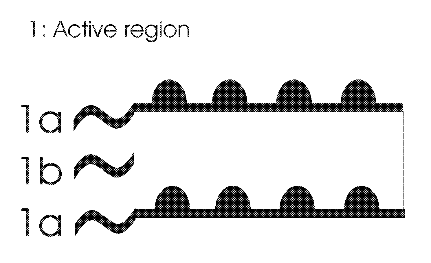
[0048]In the present invention FIG. 4 is a schematic sectional view of a device 11 with a quantum dot active layer. In this embodiment the device is a light-emitting diode 11. The device is fabricated in the (Al, Ga, In)N material system.
[0049]The light-emitting diode 11 of FIG. 4 comprises a sapphire substrate 2. The light-emitting diode 11 of FIG. 4 may contain a buffer layer 3 disposed on the substrate layer 2. The buffer layer 3 may be any orientation of (Al, Ga)N. The buffer layer may be grown by any suitable method. In the light-emitting diode 11 of FIG. 4 the buffer layer is n-type GaN.
[0050]The light-emitting diode 11 of FIG. 4 may contain an n-type (Al, Ga, In)N layer 4 grown by molecular beam epitaxy. The (Al, Ga, In)N layer 4 may use ammonia as the source of active nitrogen and be grown at 860° C. Part of the (Al, Ga, In)N layer may be grown at a lower temperature of 640° C. The (Al, Ga, In)N layer may be annealed at 860° C.
[0051]The light-emitting-diode 11 of FIG. 4 may ...
second embodiment
[0058]In a second embodiment the present invention may also be applied to the growth of a quantum dot laser diode. FIG. 5 is a schematic sectional view of a quantum dot laser diode 12 according to an embodiment of the present invention. Layers 2, 3, 4, 1a, 1bi, 1bii and 5 of the laser diode device are as already described for the light-emitting diode 11 of FIG. 4.
[0059]In addition the laser diode structure 12 of FIG. 5 may contain a first (Al, Ga, In)N cladding layer 6 disposed on the layer 4, a first (Al, Ga, In)N optical guiding layer 7 disposed on the first (Al, Ga, In)N cladding layer 6, a second (Al, Ga, In)N optical guiding layer 9 disposed over the active region 1 (on the final quantum dot layer 1a, or the final quantum dot capping layer 1bii if present) or the electron blocking layer 8 if present, and a second (Al, Ga, In)N cladding layer 10 disposed on the second GaN optical guiding layer 9.
[0060]In the laser diode 12 of FIG. 5, the first (Al, Ga, In)N cladding layer 6 and ...
PUM
 Abstract
Description
Claims
Application Information