Heat dissipating wiring board, method for manufacturing same, and electric device using heat dissipiating wiring board

a wiring board and heat dissipation technology, applied in the direction of printed electric component incorporation, electrical apparatus construction details, semiconductor/solid-state device details, etc., can solve the problem of difficult to make a finer wiring shape of lead frame 202 by press work, 0.5 mm, etc., to achieve efficient heat radiation, high density, and efficient cooling

Inactive Publication Date: 2009-10-29
PANASONIC CORP
View PDF7 Cites 14 Cited by
  • Summary
  • Abstract
  • Description
  • Claims
  • Application Information

AI Technical Summary

Benefits of technology

[0011]With the above structure, a heat radiating wiring board of the invention uses a circuit pattern constituted of a metal wiring plate where the thickness is partially thin. Therefore, if a heat generating electronic component such as an LED is mounted on a thin portion, heat is transmitted to a thick portion integrated with the thin portion. This enables efficient heat radiation. Alternatively, if a thick portion is used for a part for an LED and the like in which a high current and heat radiation are required whereas a thin portion is used for a part in which surface mounting of a circuit component such as a semiconductor or a chip component at a high density is required, the flowing of a high current of several tens to 100 A or more as for the LED and the like can be accepted in the thick portion and the LED can be efficiently cooled by utilizing the thickness of the thick portion. Further, a semiconductor component and the like to control the LED and the like can be mounted in the vicinity of the LED and the like at a high density by utilizing the thin portion. Thus, the LED and the like and their peripheral circuit components and the like can be mounted on one heat radiating wiring board, and therefore unitization and modularization, e.g., of LEDs become possible. Size reduction and cost reduction of products become possible.

Problems solved by technology

This temperature rise poses a large problem.
However, if lead frame 202 is made thick, it becomes difficult to make lead frame 202 in a finer wiring shape by press working.
It is very difficult with a thickness of 0.5 mm to make a fine pattern such as a pattern having a pattern width of 0.3 mm or 0.4 mm.
However, in a conventional high heat radiating board, since its circuit pattern constituted of lead frame 202 is a non-dense pattern provided for a high current, a dense pattern for mounting a semiconductor and the like cannot be formed.
Therefore, the conventional structure has a problem that it is difficult to mount a semiconductor circuit component for driving LED 206 together with LED 206 on the same board.

Method used


Image

  • Heat dissipating wiring board, method for manufacturing same, and electric device using heat dissipiating wiring board
  • Heat dissipating wiring board, method for manufacturing same, and electric device using heat dissipiating wiring board
  • Heat dissipating wiring board, method for manufacturing same, and electric device using heat dissipiating wiring board

Examples


first embodiment

[0045]A first embodiment is described with reference to the drawings.

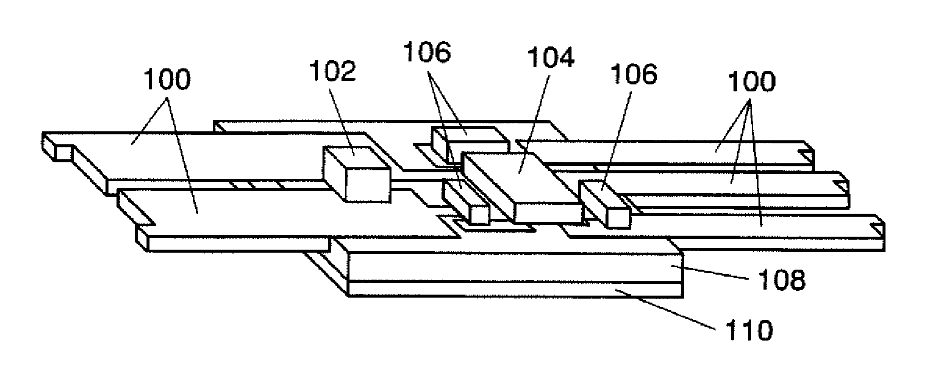
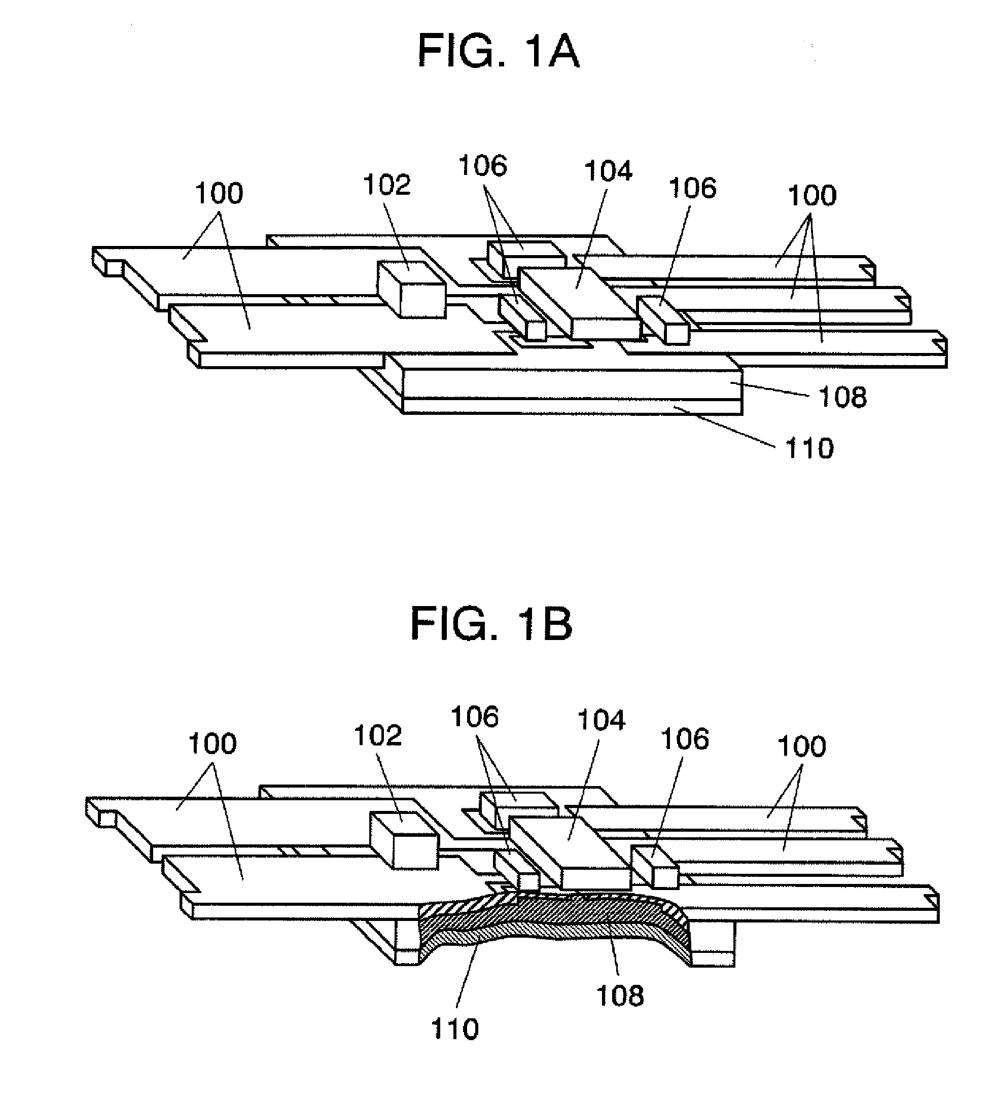
[0046]FIG. 1A is a perspective view in the state where an LED is mounted on a heat radiating wiring board in a first embodiment. FIG. 1B is a partially sectional view of FIG. 1A.

[0047]In FIG. 1A, a high-heating, high-current element such as LED 102 is mounted on different thickness lead frame 100 used as a circuit pattern. Control IC 104 for controlling LED 102 and chip component 106 are mounted on the same different thickness lead frame 100. Different thickness lead frame 100 is integrated with heat sink 110 disposed on the lower surface of this composite resin plate 108 with composite resin plate 108 interposed therebetween. This heat sink 110 is attached to composite resin plate 108 while being non-conducting with different thickness lead frame 100. Note that terminal electrodes for mounting such as LED 102 and control IC 104 are not illustrated. Needless to say, the configuration illustrated in FIGS. 1A and 1B ...

second embodiment

[0072]As a second embodiment, one example of a method for manufacturing a heat radiating wiring board using a different thickness lead frame will be described below with reference to FIGS. 3A, 3B, 4, and 5.

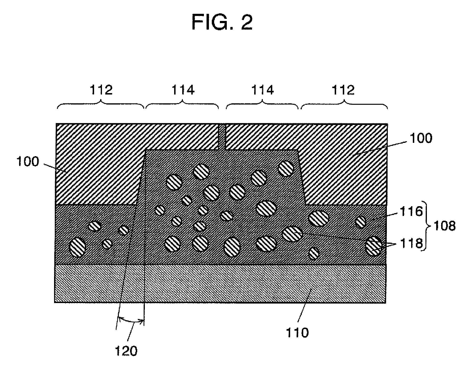
[0073]FIGS. 3A and 3B are perspective views explaining how to make different thickness lead frame 100; FIG. 3A illustrates the state of copper material 122 before pressing, FIG. 3B illustrates the state of copper material 122 after pressing. In FIG. 3A, copper material 122 is successive, irregular-shaped copper strips made by, e.g., roll forming of a thin plate mainly made of copper. Then, as illustrated in FIG. 3B, this copper material 122 is formed in a predetermined shape by pressing. Here, pressing is preferably carried out from the back side to the front side (from the lower side to the upper side in FIG. 3B). This allows a burr produced during pressing to escape to the front side (further can increase the effect of air permeability stainproof film 124 in FIG. 5 to be describ...

third embodiment

[0078]As a third embodiment, one example of optimum mounting of various electronic components onto a heat radiating wiring board will be described below with reference to FIGS. 6 to 8. FIG. 6 is a perspective view explaining a position for mounting a component on a heat radiating wiring board.

[0079]In FIG. 6, thick portion 112 of different thickness lead frame 100 is excellent in high current and heat radiation. This portion preferably constitutes high current heat radiation portion 128 such that power component 134 such as LED is mounted on the portion. On the other hand, fine and complex wiring can be formed on thin portion 114 of different thickness lead frame 100, and therefore thin portion 114 is optimum as signal circuit portion 130 and suitable for mounting of control component 132.

[0080]A tin plating process with a nickel underplate is applied to the surface (component mounting surface) of different thickness lead frame 100 in FIG. 6. In this way, tin plating and solder plat...


PUM

PropertyMeasurementUnit
thicknessaaaaaaaaaa
thicknessaaaaaaaaaa
thicknessaaaaaaaaaa

Abstract

It is an object to improve a conventional point that mounting an electronic component that requires a high current and heat radiation, such as an LED, together with other general electronic components on the same board has been difficult. To achieve this object, a different thickness lead frame partially having different thicknesses is used. On a thick portion of the different thickness lead frame, a special electronic component, such as an LED, for which a high current and heat radiation are required is mounted. Further, a thin portion of the different thickness lead frame is formed at a fine pitch, and general electronic components are mounted at a high density on the thin portion. Thus, unitization or modularization of electronic components for which a high current and heat radiation are required becomes possible.

Description

TECHNICAL FIELD[0001]The present invention relates to a heat radiating or dissipating wiring board and a manufacturing method therefor, and an electrical apparatus or device using the heat radiating or dissipating wiring board.BACKGROUND ART[0002]In recent years, as higher performance and size reduction of electronic apparatuses have been demanded, producing electronic components with higher density and higher performance have been further demanded. By making electronic components smaller, high-functional, and more effective to address such demands, their temperature rises. This temperature rise poses a large problem. A method for increasing heat radiation of an electronic component has therefore become important. Description will be given below taking a light emitting diode (LED) as an example of the electronic component for which heat generation is problematic.[0003]Among electronic components, an LED has characteristics that the amount of light emission decreases when the tempera...

Claims


Application Information

Patent Timeline
Patent Type & Authority Applications(United States)
IPC IPC(8): H05K1/00H05K1/05H05K1/16H01K3/10
CPCH01L23/142Y10T29/49128H01L23/3735H01L33/642H01L33/647H05K1/0203H05K1/056H05K3/202H05K2201/0209H05K2201/09736H05K2201/10106H01L2924/0002H01L23/145Y10T29/49162H01L2924/00H01L23/49861
Inventor TSUMURA, TETSUYANISHIYAMA, HIROHARUTSUJIMOTO, ETSUO
Owner PANASONIC CORP
Why Eureka
Try Eureka