
Method for manufacturing light-emitting device

a technology of light-emitting devices and manufacturing methods, which is applied in the direction of solid-state devices, vacuum evaporation coatings, coatings, etc., can solve the problems of high probability of decomposition or deterioration of the material which forms the transfer layer, high probability of high uneven transfer film formation, and low film quality. , to achieve the effect of high light-emitting characteristics, high accuracy and high definition

Inactive Publication Date: 2009-10-29
SEMICON ENERGY LAB CO LTD
View PDF29 Cites 10 Cited by
  • Summary
  • Abstract
  • Description
  • Claims
  • Application Information

AI Technical Summary

Benefits of technology

[0013]Then, an embodiment of the present invention is to provide a method for manufacturing a light-emitting device with high definition, high light-emitting characteristics, and a long lifetime by using a method with which a material layer which is to be a transfer layer is prevented from being evaporated beyond necessity, a desired evaporation pattern can be formed, and deterioration of a material or the like is hardly caused in performing transfer.
[0024]In a method for manufacturing a light-emitting device according to an embodiment of the present invention, a material layer over an evaporation donor substrate can be patterned and can be deposited onto a deposition target substrate by performing light irradiation twice. Specifically, the material layer formed over the evaporation donor substrate is patterned by first light irradiation, and the material layer which is patterned is evaporated onto the deposition target substrate by second light irradiation; thus, the material layer can be evaporated with high accuracy, and a light-emitting device with high definition, high light-emitting characteristics, and a long lifetime can be manufactured.
[0025]Note that, in the first light irradiation, by using laser light having a wavelength (λ1) which is reflected by the function layer, high light intensity can be instantaneously given to a desired position; thus, a pattern with high accuracy can be formed. Further, in the second light irradiation, by using light having a wavelength (λ2) which is transmitted through the function layer, the material layer which is patterned at a position overlapping with the function layer can be efficiently evaporated onto the deposition target substrate.
[0026]Note that, in the second light irradiation, in the case where a lamp is used as a light source, deposition can be performed on a large area at a time; thus, productivity of the light-emitting device can be improved. Further, in an embodiment of the present invention, by directly or indirectly heating the evaporation donor substrate instead of the second light irradiation, an evaporation material over the evaporation donor substrate can be sublimated and deposited onto the deposition target substrate.

Problems solved by technology

On the other hand, if the transfer substrate is instantaneously irradiated with laser light having high output power for shortening irradiation time with laser light, although only the transfer layer over the low-reflective layer is transferred and a desired evaporation patterning can be formed, a material which forms the transfer layer is likely to be decomposed or deteriorated because the transfer layer reaches high temperature at the moment of irradiation with laser light.
Further, a transferred film formed as described above is highly likely to be highly uneven and have low film quality.

Method used


Image

  • Method for manufacturing light-emitting device
  • Method for manufacturing light-emitting device
  • Method for manufacturing light-emitting device

Examples


embodiment 1

[0042]In Embodiment 1, a deposition method using an evaporation donor substrate according to an embodiment of the present invention is described. Note that the case where an EL layer of a light-emitting element is formed using an evaporation donor substrate over which an evaporation material is patterned will be described in Embodiment 1.

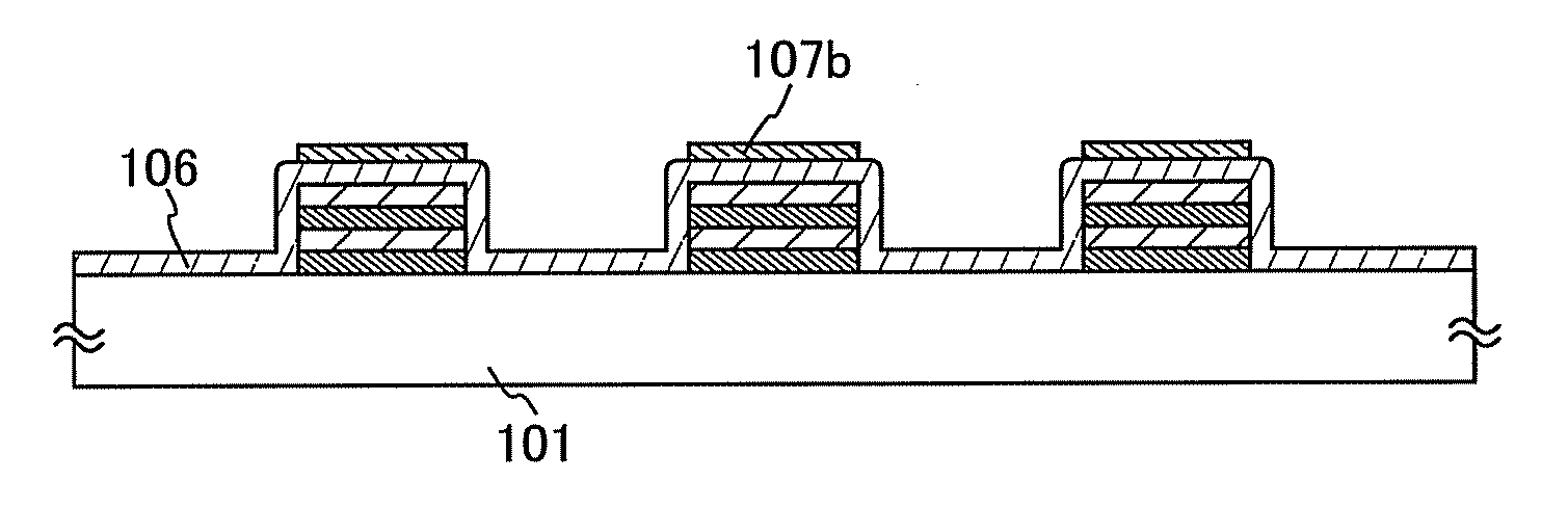
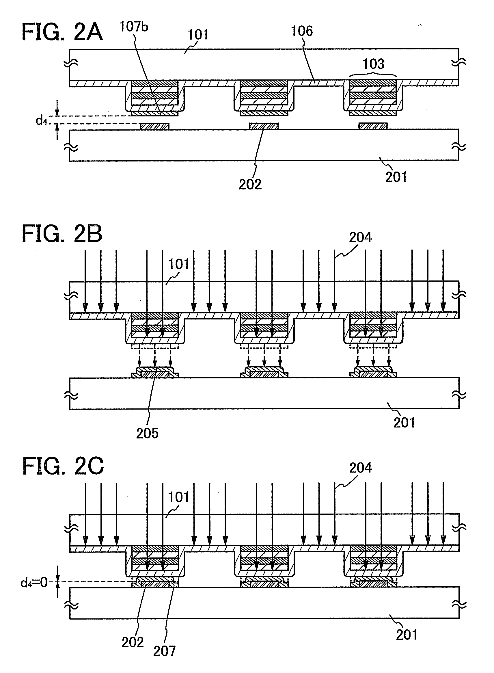
[0043]An evaporation donor substrate used in this embodiment is described with reference to FIGS. 1A to 1D. As illustrated in FIG. 1A, a function layer 103 having opening portions 102 is formed over a first substrate 101 which is a supporting substrate. Note that the function layer 103 has a structure in which high-refractive index films 104 formed with a material having a high refractive index and low-refractive index films 105 formed with a material having a low refractive index are alternately stacked. Note that the function layer 103 has a structure in which two or more high-refractive index films 104 (104a, 104b) and two or more low-refractive ...

embodiment 2

[0090]In this embodiment, in a deposition method using an evaporation donor substrate according to an embodiment of the present invention, an apparatus is described which is used in the case where an evaporation donor substrate is irradiated with laser light as the first light.

[0091]FIG. 4 is a perspective view illustrating an example of an apparatus using laser light. Laser light is outputted from a laser 403 (a YAG laser device, an excimer laser device, or the like) and transmitted through a first optical system 404 for changing a laser beam shape into a rectangular shape, a second optical system 405 for shaping the laser beam, and a third optical system 406 for collimating the laser beam; and an optical path is bent in a direction perpendicular to a first substrate 401, which is an evaporation donor substrate, over a first substrate stage 409 by using a reflecting mirror 407. Then, the first substrate 401 is irradiated with the laser beam.

[0092]Note that a structure of the evapor...

embodiment 3

[0101]In this embodiment, in a deposition method using an evaporation donor substrate according to an embodiment of the present invention, an apparatus which is used in the case where an evaporation donor substrate including a material layer which is patterned is irradiated with lamp light as the second light is described.

[0102]In FIG. 5A, a deposition chamber 501 is a vacuum chamber and is connected to another chamber via a gate valve 502. Further, the deposition chamber 501 is provided with an exhaust mechanism 503. In addition, in the deposition chamber 501, at least a substrate stage 504 for holding a first substrate 511 (including material layers 513) which is an evaporation donor substrate, substrate supporting units 505 for holding a third substrate 512 which is a deposition target substrate, and light sources 510 are provided.

[0103]Note that, over the first substrate 511 which is held by the substrate stage 504, the material layer is patterned by performing treatment shown i...


PUM

PropertyMeasurementUnit
refractive indexaaaaaaaaaa
reflectanceaaaaaaaaaa

Abstract

By irradiating a first substrate which is an evaporation donor substrate including a function layer in which films having different refractive indexes (high-refractive index films and low refractive index films) are stacked with first light (wavelength=λ1), a material layer over the first substrate is patterned, and by irradiating the first substrate with second light (wavelength=λ2) which is different from λ1, the material layer which is patterned is evaporated onto a second substrate which is a deposition target substrate.

Description

BACKGROUND OF THE INVENTION[0001]1. Field of the Invention[0002]The present invention relates to a method for manufacturing a light-emitting device using an evaporation method.[0003]2. Description of the Related Art[0004]Light-emitting elements, which use organic compounds as a light emitter and are characterized by the thinness, lightweight, fast response, and direct current low voltage driving, are expected to be applied to next-generation flat panel displays. In particular, display devices in which light-emitting elements are arranged in matrix have been considered to be superior to conventional liquid crystal display devices in terms of a wide viewing angle and excellent visibility.[0005]It is considered that a light emission mechanism of a light-emitting element is as follows: when voltage is applied between a pair of electrodes which interpose an EL layer, electrons injected from a cathode and holes injected from an anode are recombined in the light emission center of the EL l...

Claims


Application Information

Patent Timeline
Patent Type & Authority Applications(United States)
IPC IPC(8): B05D5/06
CPCH01L27/3211H01L51/56H01L51/0013C23C14/048H10K59/35H10K71/18H10K71/441H10K71/60H10K71/00
Inventor IKEDA, HISAOIBE, TAKAHIRO
Owner SEMICON ENERGY LAB CO LTD
Features
  • Generate Ideas
  • Intellectual Property
  • Life Sciences
  • Materials
  • Tech Scout
  • Unparalleled Data Quality
  • Higher Quality Content
  • 60% Fewer Hallucinations
Learn More