Pad-assisted electropolishing

a technology of electropolishing and metal-containing surfaces, applied in the field of integrated circuit fabrication, can solve the problems of forming concave or depressions, affecting the quality of the surface of the metal and the dielectric surface, and damaging the fragile low-k dielectric surface, so as to avoid etching, erosion, and other damage to the metal and dielectric surface. , the effect of avoiding etching

Inactive Publication Date: 2009-11-12
NOVELLUS SYSTEMS
View PDF47 Cites 9 Cited by
  • Summary
  • Abstract
  • Description
  • Claims
  • Application Information

AI Technical Summary

Benefits of technology

[0022]The invention helps to solve some of the problems mentioned above by providing systems and methods for pad-assisted electropolishing of integrated circuit substrates. Embodiments in accordance with the invention utilize novel electrical edge-contact techniques that allow planarization of the entire surface of the substrate, including extreme peripheral areas at the outside edge of wafer. Pad-assisted electropolishing in accordance with the invention avoids dishing, erosion, and scratching or other damage to metal and dielectric surfaces.
[0026]Methods in accordance with the invention allow use of a simple, low-cost isotropic wet-etching technique after pad-assisted electropolishing that selectively removes remains of copper and typically is stopped at a barrier / etch-stop layer. A feature of embodiments of methods in accordance with the invention is the capability of planarizing the entire surface of the substrate face, including extreme peripheral portions of the substrate face contiguous to the side edges of the substrate.
[0028]Thus, methods and apparatus in accordance with the invention allow substantial uncoupling of physical buffing processes from electrochemical processes being conducted on a substrate wafer.

Problems solved by technology

The use of advanced “bottom-up” electrofilling techniques with wafers having low and high aspect-ratio features has created a problem of deposited metal surfaces with a wide range of topography, that is, topography containing both recessed and raised areas.
Therefore, while electroplating is the preferred method of metalization, various aspects of improved plating regimens create challenging topography for subsequent planarization.
The large downward pressure exerted onto a wafer during typical CMP polishing may damage fragile low-k dielectrics.
Overpolishing of some materials can result, however, in the formation of topographical defects, such as concavities or depressions in features, referred to as dishing.
As a consequence, unwanted static etching of the metallic features of the polished surface can occur, resulting in dishing.
Dishing typically results in a height differential between the dielectric oxide layer and metalization features.
Increased resistivity can lead to overheating that causes the semiconductor device to fail.
Another problem of CMP processes is excessive removal of material from a wafer.
Erosion can lead to a non-planar topography across the wafer that can cause short circuits to form in subsequently deposited metal layers.
Additional problems of CMP include scratching of fine-lined metal in dielectric features by the agglomerations of abrasive particles.
Scratching results in damage to interconnects and yield losses.
A conglomerate of particles and gels can be removed from the slurries using point of use filtration prior to substrate polishing; however, plugging of the filters requires interruption of the process for filtrate removal, which is expensive and results in lower production.
This method requires either large shear force and / or the presence of abrasives in order to achieve a reasonable removal rate, which may result in damage to the wafer, scratches, oxide erosion and copper dishing.
Unfortunately, CMP polishing techniques are difficult to control; the endpoint can be difficult to detect.
Also, CMP materials and equipment are expensive.
The high equipment cost, waste handling cost, and low throughput contribute to the overall expense of CMP.
Also, with the introduction of low-k dielectrics into chip production, modification of traditional CMP processes is required, as current methods result in cracking and the lamination of most dielectric materials, which have a low compression strength and are fragile.
A problem arises during the electropolishing of surfaces in which a large number of low aspect-ratio (larger width than depth) features exist.
Depositing a thick metal layer would be uneconomical due to necessary removal of the large excess of metal at a later stage.
Obviously this is an unacceptable result.

Method used


Image

  • Pad-assisted electropolishing
  • Pad-assisted electropolishing
  • Pad-assisted electropolishing

Examples


Embodiment Construction

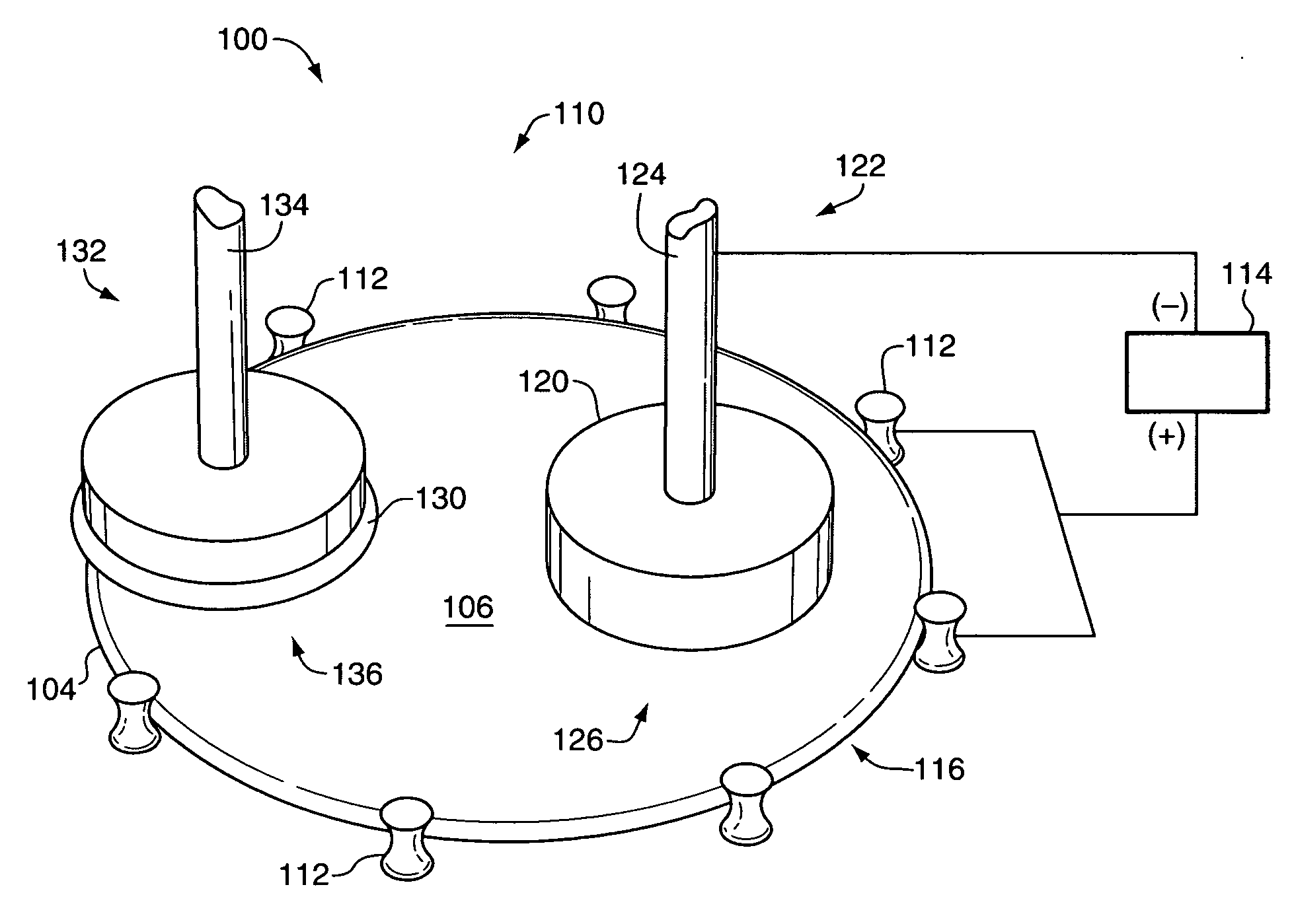
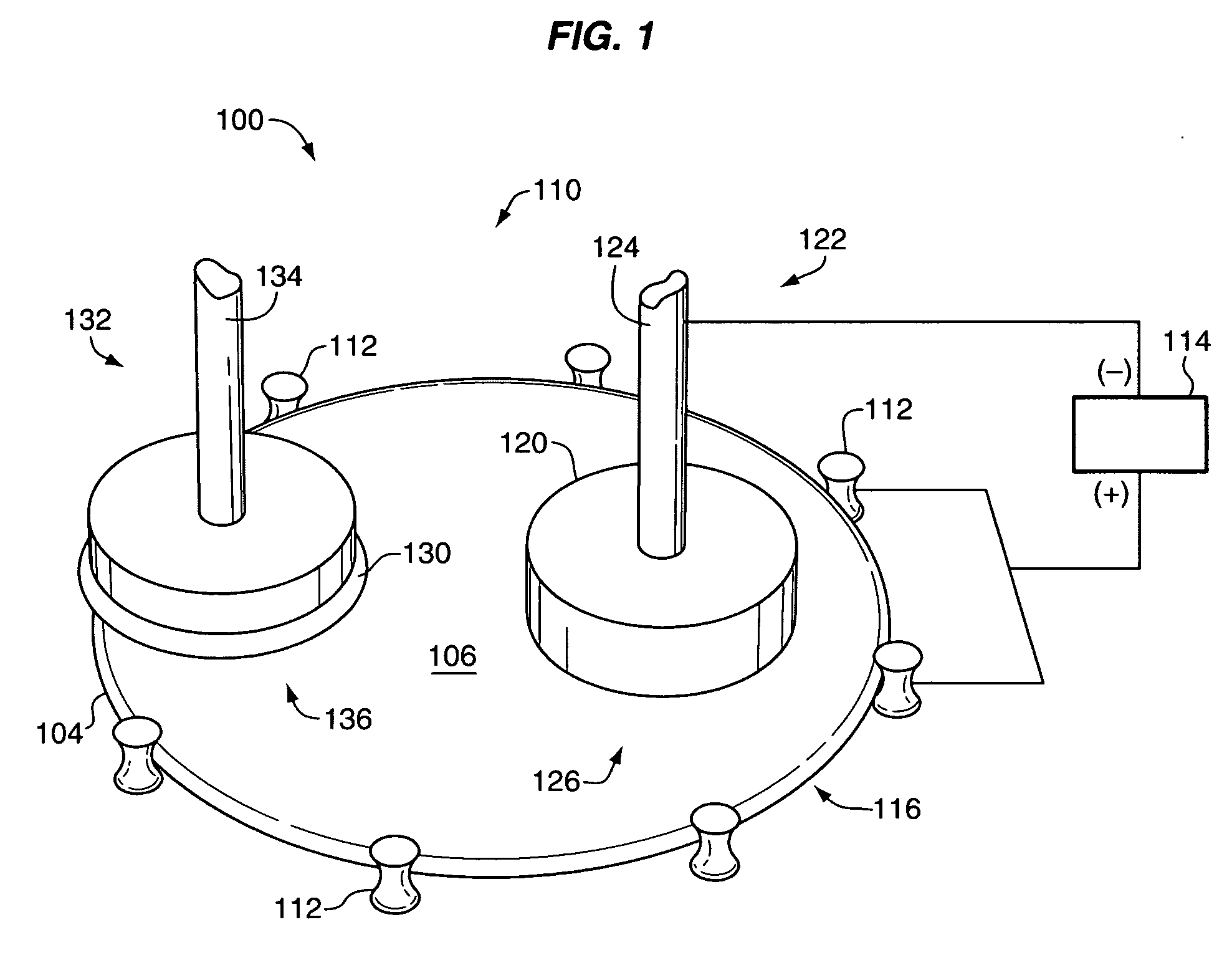
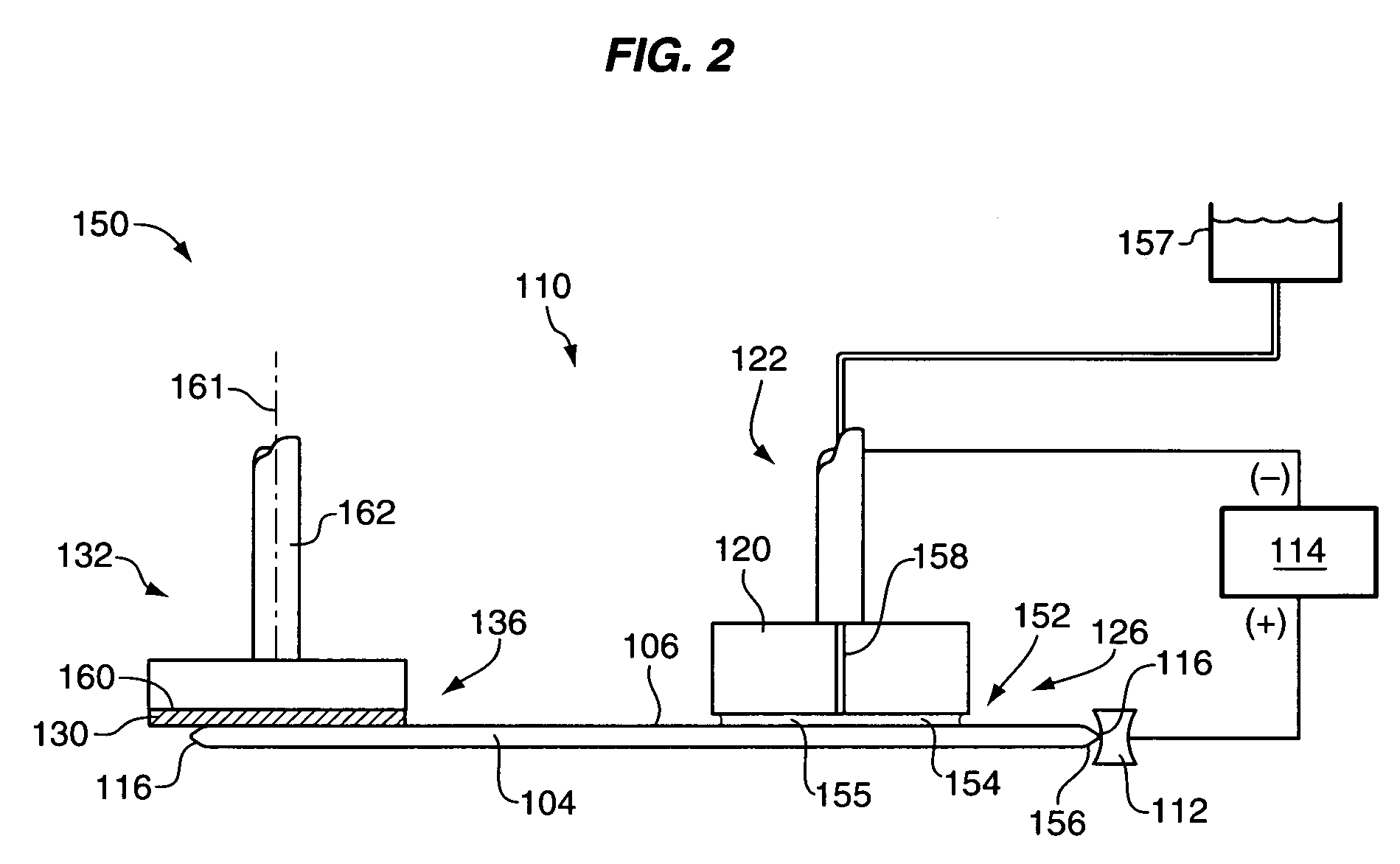
[0053]The invention is described herein with reference to FIGS. 1-22. It should be understood that the structures and systems depicted schematically in FIGS. 1-11, 13-21 serve explanatory purposes and are not precise depictions of actual structures and systems in accordance with the invention. For example, the depiction of power supplies and fluid handling in the figures below likely is different from hardware in actual embodiments. Furthermore, the embodiments described herein are exemplary and are not intended to limit the scope of the invention, which is defined in the claims below. For the sake of clarity, parts and elements of various embodiments having similar structure and function are identified using the same reference numerals in the figures below.

[0054]In this specification, terms of orientation, such as “face-up”, “above”, “below”, “up”, “down”, “top”, “bottom”, and “vertical” used to describe embodiments relate to the relative directions in FIGS. 1-11, and 13-21, in whi...


PUM

PropertyMeasurementUnit
timeaaaaaaaaaa
time periodaaaaaaaaaa
thicknessaaaaaaaaaa

Abstract

Pad-assisted electropolishing of the substrate is conducted by performing anodic dissolution of metal at a first portion of the substrate and simultaneously mechanically buffing a second portion of the substrate with a buffing pad. Anodic dissolution includes forming a thin liquid layer of electropolishing liquid between the anodic substrate and a cathodic electropolishing head. The location of electrical contacts between the substrate and power supply allow peripheral edge regions of the substrate to be mechanically buffed with the pad. Preferably, a substrate is further planararized using an isotropic material-removal technique. An apparatus includes an electropolishing head that is movable to a position proximate to a first portion of a substrate to form a thin gap, and a buffing pad that mechanically buffs a second portion of the substrate using minimal pressure.

Description

RELATED APPLICATIONS[0001]This application is a continuation-in-part application, claiming priority under 35 USC 120, of co-owned and co-pending U.S. patent application Ser. No. 10 / 609,518, filed Jun. 30, 2003, by Mayer et al., having the title “Liquid Treatment Using Thin Liquid Layer”, which claimed the benefit of U.S. Provisional Application Ser. No. 60 / 392,203, filed Jun. 28, 2002. This application is also a continuation-in-part application, claiming priority under 35 USC 120, of co-owned and co-pending U.S. patent application Ser. No. 10 / 739,822, filed Dec. 17, 2003, by Mayer et al., having the title “Method for Planar Electroplating”, which is a continuation-in-part of U.S. patent application Ser. No. 09 / 967,075, filed Sep. 28, 2001 by Mayer et al., titled “Method And Apparatus For Uniform Electropolishing of Damascene IC Structures By Selective Agitation,” now issued U.S. Pat. No. 6,709,565, which in turn was a continuation-in-part of U.S. patent application Ser. No. 09 / 412,8...

Claims


Application Information

Patent Timeline
Patent Type & Authority Applications(United States)
IPC IPC(8): B23H5/08
CPCC25F3/30H01L21/6715H01L21/32125H01L21/32115
Inventor MAYER, STEVEN T.SVIRCHEVSKI, JULIADREWERY, JOHN STEPHEN
Owner NOVELLUS SYSTEMS
Why Eureka
Try Eureka