Mis field effect transistor and method for manufacturing the same

a field-effect transistor and field-effect technology, applied in the direction of semiconductor devices, basic electric elements, electrical appliances, etc., can solve the problems of not being able to implement a normally-off operation, not being able to achieve normal-off operation, and insufficient breakdown voltage, so as to achieve the effect of reducing the reliability of the device, reducing the mobility of the carrier in the channel region, and improving the breakdown voltag

Active Publication Date: 2009-11-12
ROHM CO LTD
View PDF11 Cites 29 Cited by
  • Summary
  • Abstract
  • Description
  • Claims
  • Application Information

AI Technical Summary

Benefits of technology

[0046]In particular, the breakdown voltage can be more effectively improved by rendering the band gaps of both of the first and third group III-V nitride semiconductor layers larger than the band gap of the second group III-V nitride semiconductor layer and forming a double heterojunction.
[0047]The gate insulating film may be brought into a structure having a group III-V nitride intrinsic semiconductor gate layer (51: preferably containing no In) containing Al. This group III-V nitride intrinsic semiconductor gate layer forms an excellent interface betwee...

Problems solved by technology

However, every one of heretofore proposed GaN devices has a lateral structure obtained by arranging a source, a gate and a drain along a substrate surface, is not necessarily suitable for a power devic...

Method used


Image

  • Mis field effect transistor and method for manufacturing the same
  • Mis field effect transistor and method for manufacturing the same
  • Mis field effect transistor and method for manufacturing the same

Examples


first embodiment

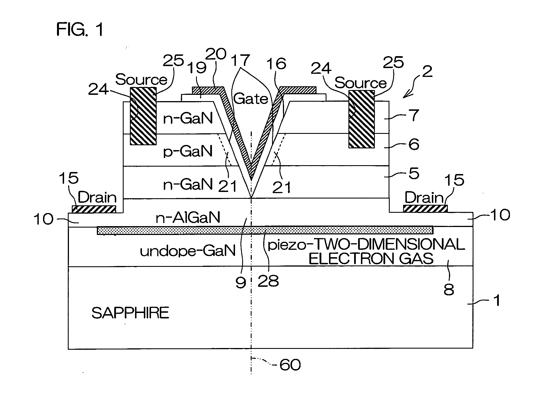
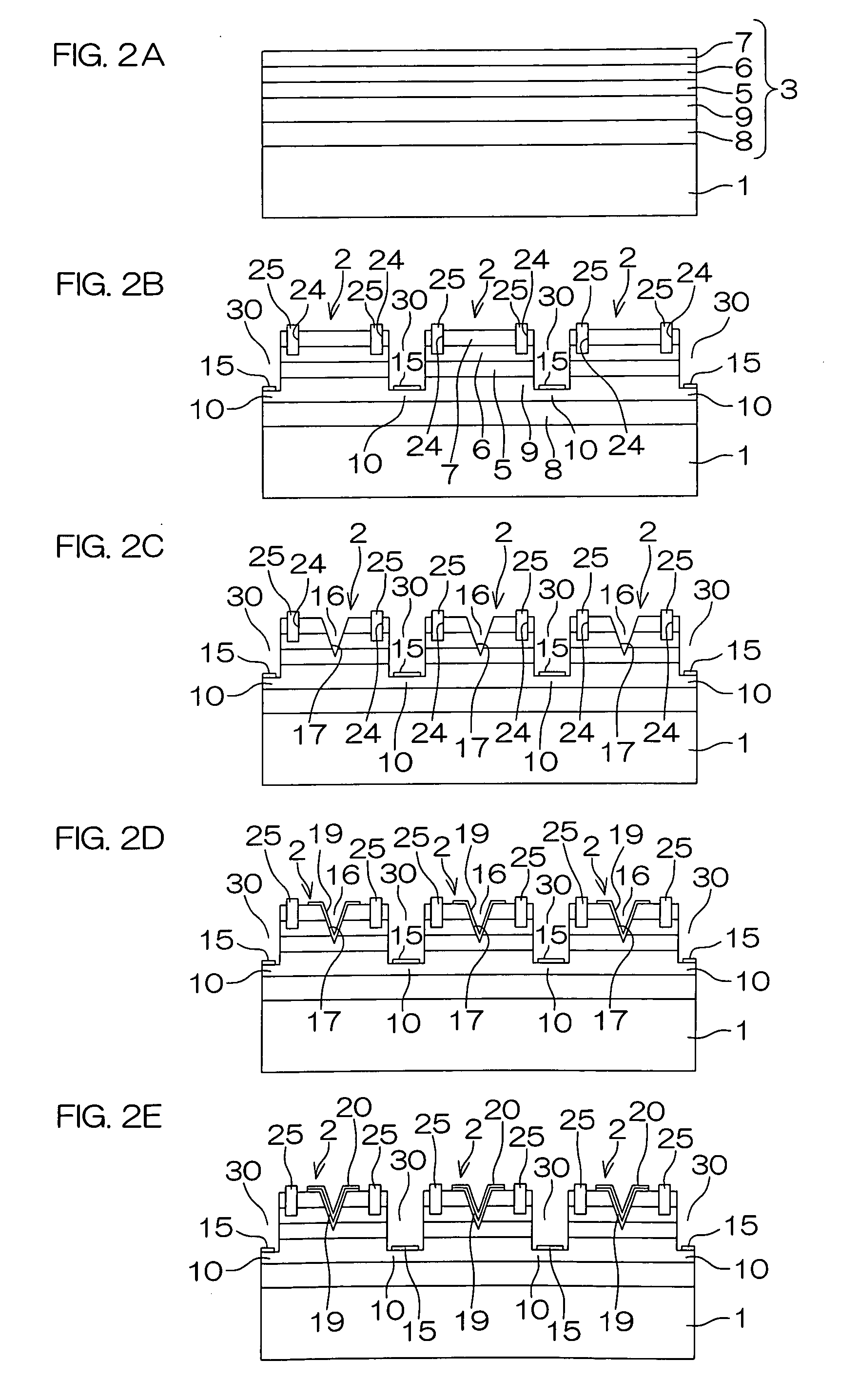
[0055]FIG. 1 is a schematic sectional view for illustrating the structure of an MIS field-effect transistor according to the present invention. This field-effect transistor includes a sapphire substrate 1 which is an insulating substrate and a nitride semiconductor multilayer structure portion 2 consisting of GaN compound semiconductor layers grown on this sapphire substrate 1. The nitride semiconductor multilayer structure portion 2 includes an N-type GaN layer 5 (drain layer), a P-type GaN layer 6 stacked on this N-type GaN layer 5 and an N-type GaN layer 7 (source layer) stacked on this P-type GaN layer 6. Further, the nitride semiconductor multilayer structure portion 2 includes an intrinsic (undoped) GaN layer 8 formed in contact with the sapphire substrate 1 and an N-type AlGaN layer 9 stacked on this intrinsic GaN layer 8, and the N-type GaN layer 5 is stacked on this N-type AlGaN layer 9.

[0056]The nitride semiconductor multilayer structure portion 2 is etched up to such a de...

second embodiment

[0083]FIG. 3 is a schematic sectional view for illustrating the structure of an MIS field-effect transistor according to the present invention. Referring to FIG. 3, reference numerals identical to those in the case of FIG. 1 are allocated to portions corresponding to the respective portions shown in the above FIG. 1. According to this embodiment, etching on both sides of a nitride semiconductor multilayer structure portion 2 is stopped in a layer-thickness intermediate portion of an N-type GaN layer 5. Thus, the N-type GaN layer 5 has drawn portions 11 drawn in the lateral direction of the nitride semiconductor multilayer structure portion 2 along the surface of a sapphire substrate 1. In other words, these drawn portions 11 are constituted of extensions of the N-type GaN layer 5. Drain electrodes 15 are formed in contact with the upper surfaces of these drawn portions 11.

[0084]Also according to this structure, an operation similar to that of the aforementioned first embodiment is e...

third embodiment

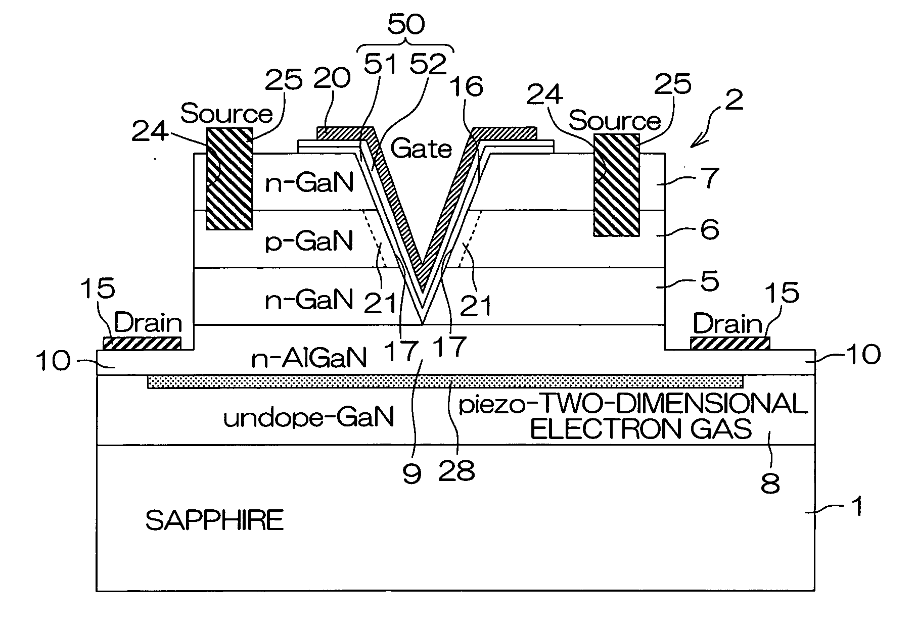
[0086]FIG. 4 is a schematic sectional view for illustrating the structure of an MIS field-effect transistor according to the present invention. Referring to FIG. 4, reference numerals identical to those in the case of FIG. 1 are allocated to portions corresponding to the respective portions shown in the above FIG. 1. According to this embodiment, a gate insulating film 50 is formed by an AlGaN regrowth layer 51 regrown (epitaxially grown) from wall surfaces 17 of a trench 16 and an insulating film 52 stacked and formed on the surface of this AlGaN regrowth layer 51. This gate insulating film 50 is formed over a region covering the wall surfaces 17 of the trench 16 and reaching edge portions of the trench 16 on the upper surface of an N-type GaN layer 7, similarly to the gate insulating film 19 in the aforementioned embodiment.

[0087]The AlGaN regrowth layer 51 is epitaxially grown from the wall surfaces 17 which are GaN crystal surfaces after forming the trench 16 by dry etching and ...


PUM


Abstract

The MIS field-effect transistor includes: a substrate; a nitride semiconductor multilayer structure portion formed on the substrate, including a first group III-V nitride semiconductor layer of a first conductivity type, a second group III-V nitride semiconductor layer of a second conductivity type stacked thereon and a third group III-V nitride semiconductor layer of the first conductivity type stacked thereon; a gate insulating film formed on a wall surface formed over the first, second and third group III-V nitride semiconductor layers to extend over these first, second and third group III-V nitride semiconductor layers; a gate electrode made of a conductive material formed as being opposed to the second group III-V nitride semiconductor layer via the gate insulating film; a drawn portion electrically connected to the first group III-V nitride semiconductor layer and drawn from the nitride semiconductor multilayer structure portion in a direction parallel to the substrate; a drain electrode formed in contact with the drawn portion; and a source electrode electrically connected to the third group III-V nitride semiconductor layer.

Description

TECHNICAL FIELD[0001]The present invention relates to an MIS field-effect transistor employing group III-V nitride semiconductors and a method of manufacturing the same.PRIOR ART[0002]In general, a power device employing a silicon semiconductor is employed for a power amplifier circuit, a power supply circuit, a motor driving circuit or the like.[0003]However, improvement in breakdown voltage, reduction in resistance and improvement in speed of a silicon device are now reaching the limits due to the theoretical limit of the silicon semiconductor, and it is becoming difficult to satisfy requirements of the market.[0004]Therefore, development of a GaN device having characteristics such as a high breakdown voltage, a high-temperature operation, a high current density, high-speed switching and small on-resistance is examined (see following Non-Patent Document 1).Patent Document 1: Japanese Unexamined Patent Publication No. 2004-260140Patent Document 2: Japanese Unexamined Patent Publica...

Claims


Application Information

Patent Timeline
IPC IPC(8): H01L29/78
CPCH01L21/28587H01L29/0856H01L29/0873H01L29/2003H01L29/205H01L29/802H01L29/4236H01L29/432H01L29/66734H01L29/7787H01L29/7813H01L29/41766
Inventor OHTA, HIROAKITAKASU, HIDEMI
Owner ROHM CO LTD
Why Eureka
Try Eureka