Solid-state image pickup device and electronic apparatus

Active Publication Date: 2009-11-12
SONY SEMICON SOLUTIONS CORP
View PDF8 Cites 51 Cited by
  • Summary
  • Abstract
  • Description
  • Claims
  • Application Information

AI Technical Summary

Benefits of technology

[0027]The solid-state image pickup device according to an embodiment of the present invention includes the trench to be formed into the optical waveguide, in which the trench reaches the etching stopper film, i.e., the trench does not pass through the etching stopper film. Furthermore, the etching stopper film is composed of silicon carbide, arranged adjacent to the semiconductor substrate, and distant from the lowermost wiring among the wirings embedded in the insulating film, thereby further improving the characteristics such as dark current and bright defects, increasing the sensitivity, and reducing the amount of color mixing.
[0028]The electr

Problems solved by technology

Solid-state image pickup devices including optical waveguides have a problem of the difficulty in further improving the ch

Method used


Image

  • Solid-state image pickup device and electronic apparatus
  • Solid-state image pickup device and electronic apparatus
  • Solid-state image pickup device and electronic apparatus

Examples


first embodiment

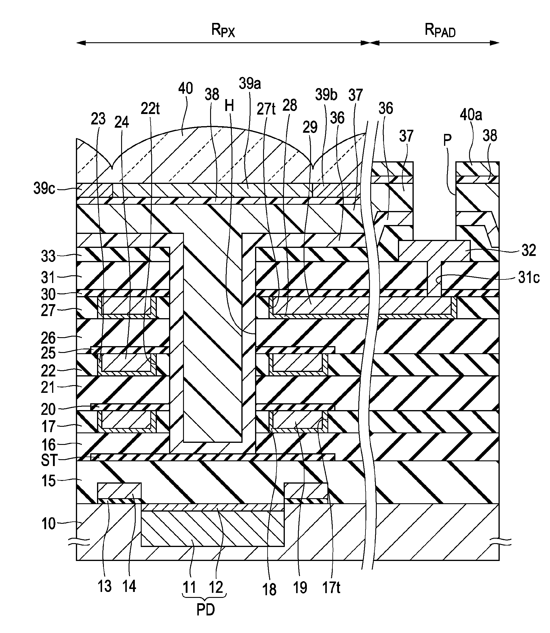
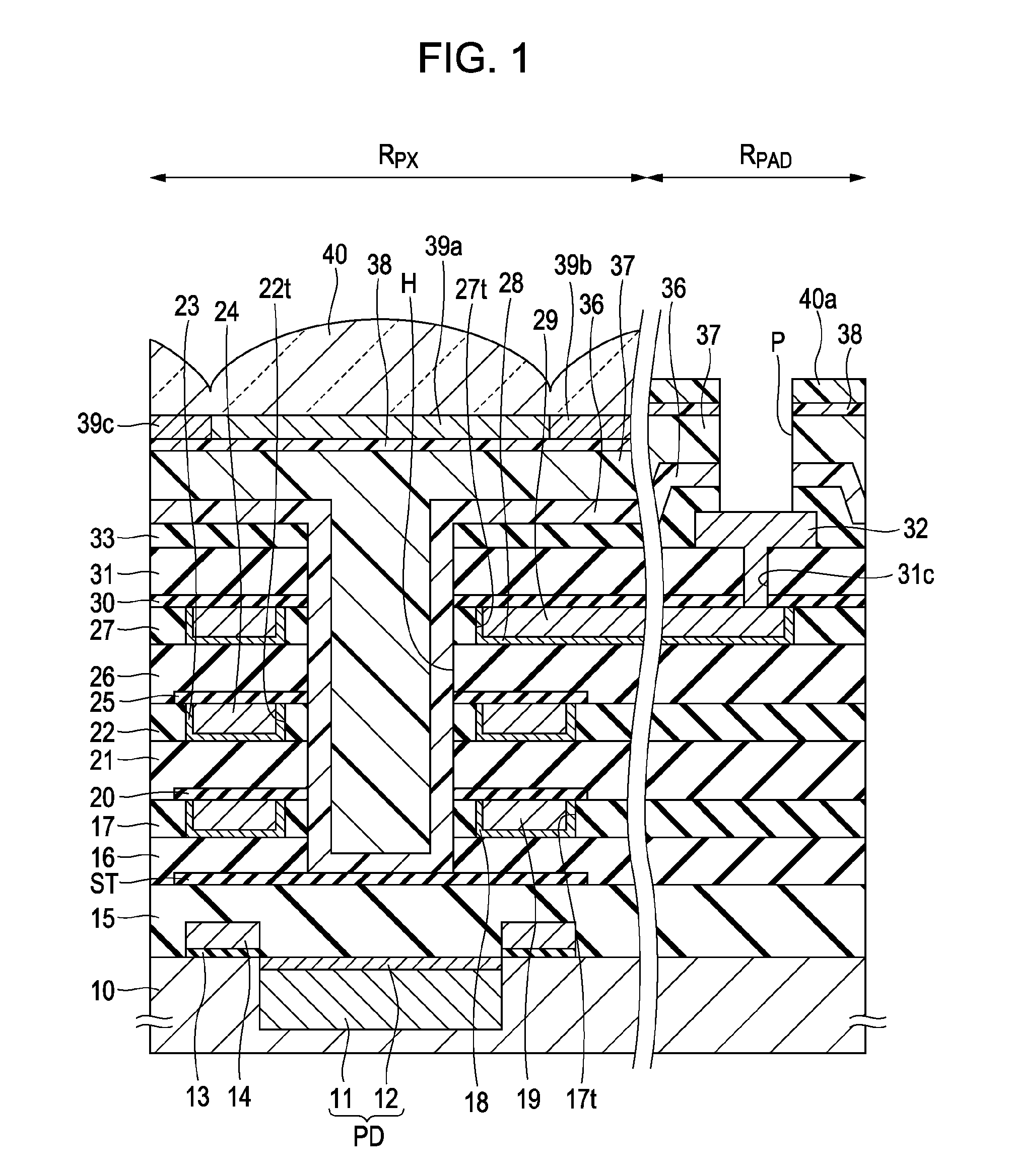
[0040]FIG. 1 is a schematic cross-sectional view of a CMOS sensor which is a solid-state image pickup device including a plurality of pixels according to this embodiment, and shows a pixel region RPX and a pad electrode region RPAD.

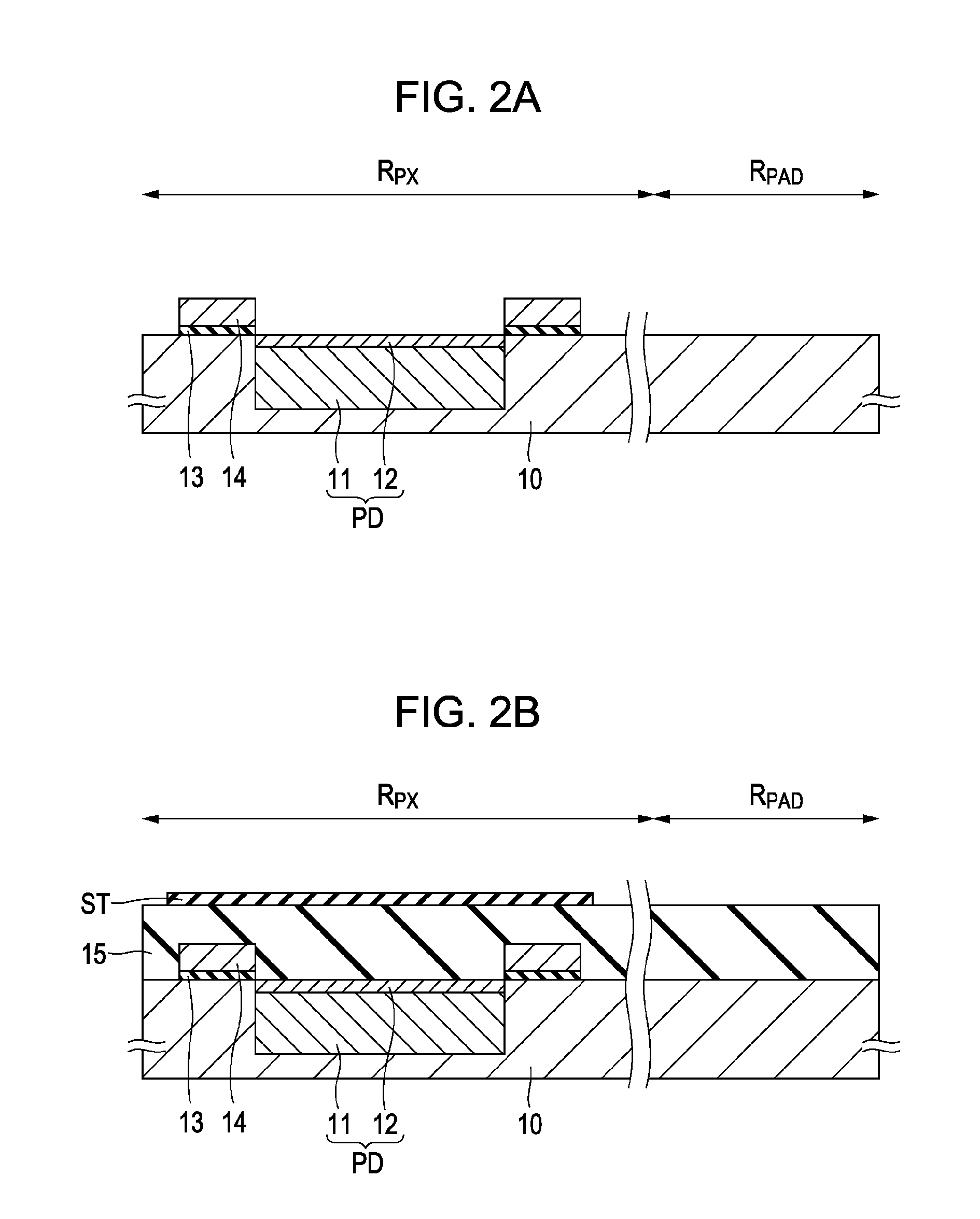
[0041]For example, in the pixel region RPX serving as a light-incident surface, an n-type charge accumulation layer 11 and a p+-type surface layer 12 serving as its surface layer are formed in a p-well area of a semiconductor substrate 10 in each of the pixels, thereby forming a photodiode PD having a pn junction. A gate insulating film 13 and a gate electrode 14 are arranged adjacent to the photodiode PD on the semiconductor substrate.

[0042]For example, a signal reading section including floating diffusion and a CCD charge transfer channel is arranged on the semiconductor substrate, the signal reading section being configured to read a signal charge or a voltage in response to a signal charge generated and accumulated in the photodiode PD. Thereby, the a...

example 1

[0114]According to the first embodiment, a CMOS sensor (a) having the structure in which the etching stopper film ST was located as close as possible to the semiconductor substrate to reduce the distance between the photodiode and the optical waveguide was produced. Here, the passivation film was composed of SiN.

[0115]A CMOS sensor (b) was produced as in the CMOS sensor (a), except that the etching stopper film was not formed and that the trench to be formed into an optical waveguide was formed so as to reach the first diffusion preventing film.

[0116]Sensitivities of the CMOS sensors were measured. FIG. 8 shows the results.

[0117]FIG. 8 shows plots of the sensitivities of the CMOS sensors (a) and (b) against the F number.

[0118]The sensitivity of the CMOS sensor (a) was 10% to 30% larger than that of the CMOS sensor (b) in the entire range of the F number. The results demonstrated that a reduction in the distance between the photodiode and the optical waveguide by locating the etching...

example 2

[0119]According to the first embodiment, a CMOS sensor (a) having the structure in which the etching stopper film ST was located as close as possible to the semiconductor substrate to reduce the distance between the photodiode and the optical waveguide was produced. Here, the passivation film was composed of SiN.

[0120]A CMOS sensor (b) was produced as in the CMOS sensor (a), except that the passivation film was composed of SiON.

[0121]A CMOS sensor (c) was produced as in the CMOS sensor (a), except that the etching stopper film was not formed and that the trench to be formed into an optical waveguide was formed so as to reach the first diffusion preventing film.

[0122]Color mixing ratios of the CMOS sensors were measured. FIG. 9 shows the results.

[0123]FIG. 9 shows plots of the color mixing ratios of the CMOS sensors (a), (b), and (c) against the incident angle.

[0124]The color mixing ratios of the CMOS sensors (a) and (b) were lower than that of the CMOS sensor (c). The results demons...


PUM


Abstract

A solid-state image pickup device includes a semiconductor substrate having a light-incident surface, a plurality of pixels arranged on the light-incident surface, a photodiode arranged in each of the pixels, an insulating film arranged on the semiconductor substrate and configured to cover the photodiodes, wirings embedded in the insulating film, an etching stopper film distant from the lowermost wiring among the wirings, arranged adjacent to the semiconductor substrate, configured to cover at least a region where each of the photodiodes is arranged, and composed of silicon carbide, a trench arranged above each of the photodiodes so as to reach the etching stopper film, and an optical waveguide with which each of the trenches is filled, the optical waveguide having a higher refractive index than the insulating film.

Description

BACKGROUND OF THE INVENTION[0001]1. Field of the Invention[0002]The present invention relates to solid-state image pickup devices and electronic apparatuses. In particular, the present invention relates to a solid-state image pickup device including pixels having photodiodes on a light-incident surface, the pixels being arranged in a matrix, and relates to an electronic apparatus including the solid-state image pickup device.[0003]2. Description of the Related Art[0004]In solid-state image pickup devices such as complementary metal oxide semiconductor (CMOS) sensors and charge-coupled devices (CCDs), light is incident on photodiodes (photoelectric conversion units) arranged on surfaces of semiconductor substrates to generate signal charges in the photodiodes, resulting in image signals.[0005]In CMOS sensors, for example, photodiodes are provided in respective pixels arranged in a two-dimensional matrix on a light-incident surface. Signal charges generated and accumulated in photodio...

Claims


Application Information

Patent Timeline
IPC IPC(8): H04N5/335H04N5/225H01L21/3205H01L21/768H01L23/52H01L23/522H01L23/532H01L27/14H01L27/146
CPCH01L27/14625H01L27/14629H01L27/14685H01L27/146
Inventor TOUMIYA, YOSHINORI
Owner SONY SEMICON SOLUTIONS CORP
Why Eureka
Try Eureka