
Photosensitive glass paste and multilayer wiring chip component

a technology of multi-layer wiring and photosensitive glass, which is applied in the direction of photomechanical equipment, instruments, and semiconductor/solid-state device details, etc., can solve the problems of disadvantageous degradation of insulating properties between layers and inferior wettability, and achieve superior wettability to ceramic aggregates, low-temperature and short-time sintering

Active Publication Date: 2009-11-19
MURATA MFG CO LTD
View PDF8 Cites 10 Cited by
  • Summary
  • Abstract
  • Description
  • Claims
  • Application Information

AI Technical Summary

Benefits of technology

[0027]The photosensitive glass paste of the present invention has an inorganic component including a primary glass, a sintering aid glass, and a ceramic aggregate and a photosensitive organic component, a glass having a contact angle with the ceramic aggregate at 800° C. smaller than that of the primary glass with the ceramic aggregate at 800° C. and a softening point of 600° C. or more is used as the sintering aid glass, and the content ratio thereof in the inorganic component is set to 5 to 10 percent by volume of the inorganic component; hence, low-temperature and short-time sintering can be carried out, and generation of voids and diffusion of Ag in glass layers formed by a firing step can be suppressed.
[0007]A glass containing SiO2, B2O3, and K2O (hereinafter also referred to as “Si—B—K-based glass”), which is usable according to Patent Document 1, has low viscous fluidity during firing. Accordingly, for example, when firing a laminate of glass layers containing this Si—B—K-based glass and conductor layers containing Ag as a conductive component laminated thereto, degradation in insulating properties between the layers caused by diffusion of the conductive Ag into the glass layers (insulating layers) can be suppressed or prevented; hence, the glass described above is a preferable material for that reason.
[0029]When a sintering aid glass having a softening point of 600° C. or more is used, most organic materials, such as a binder, can be efficiently removed by a debindering step generally performed in the range of 500 to 600° C.; hence, in a subsequent firing, generation of voids caused by oxidation of carbon that remains when the glass component is softened can be efficiently suppressed or prevented.
[0030]By using the photosensitive glass paste of the present invention, when a multilayer wiring chip component, such as a multilayer inductor, having a structure in which conductor layers are provided between glass layers is manufactured, a highly reliable multilayer wiring chip component having superior interlayer insulating properties and desired properties can be efficiently manufactured.
[0031]In addition, since low-temperature and short-time firing can be performed by using the photosensitive glass paste of the present invention, glass layers (insulating layers) can be reliably formed in which via holes each having a predetermined shape and dimensional accuracy are disposed at predetermined positions.
[0033]In addition, since a glass used as the primary glass contains 70 to 90 percent by weight of SiO2, 15 to 20 percent by weight of B2O3, and 1 to 5 percent by weight of K2O has low viscous fluidity, diffusion of Ag to glass layers formed by firing can be efficiently suppressed. Hence, a glass layer (insulating layer) having high insulating properties can be formed by using the photosensitive glass paste of the present invention.
[0038]By containing a phosphorous-based compound as a photopolymerization initiator, polymerization of a photosensitive organic compound can be reliably started when via holes are formed by a photolithography method or the like, and via holes having superior shape and dimensional accuracy can be reliably formed, so that a multilayer wiring chip component having high performance and high reliability can be manufactured.
[0033]In addition, since a glass used as the primary glass contains 70 to 90 percent by weight of SiO2, 15 to 20 percent by weight of B2O3, and 1 to 5 percent by weight of K2O has low viscous fluidity, diffusion of Ag to glass layers formed by firing can be efficiently suppressed. Hence, a glass layer (insulating layer) having high insulating properties can be formed by using the photosensitive glass paste of the present invention.
[0035]When at least one selected from the group consisting of alumina, magnesia, spinel, silica, forsterite, steatite, and zirconia is contained as the ceramic aggregate in the inorganic component at a ratio of 22.5 to 27.5 percent by volume, a glass layer having a flexural strength of 160 MPa or more can be formed, and in addition, the necessary shape preservation ability can be realized, so that a multilayer structure (multilayer wiring chip component) having superior shape and dimensional accuracy can be obtained.
[0038]By containing a phosphorous-based compound as a photopolymerization initiator, polymerization of a photosensitive organic compound can be reliably started when via holes are formed by a photolithography method or the like, and via holes having superior shape and dimensional accuracy can be reliably formed, so that a multilayer wiring chip component having high performance and high reliability can be manufactured.
[0025]The phosphorous-based compound functioning as the photopolymerization initiator can be at least one selected from the group consisting of bis(2,4,6-trimethylbenzoyl)-phenylphosphine oxide, 2,4,6-trimethylbenzoyl diphenylphosphine oxide, bis(2,6-dimethoxybenzoyl)-2,4,4-trimethylpentylphosphine oxide, bis(2,6-dichlorobenzoyl)-4-propylbenzylphosphine oxide, 2,4,6-trimethylbenzoyl diphenylphosphinate, and (2,6-dimethoxybenzoyl)-2,4,4-pentylphosphine oxide.
[0040]Since the multilayer wiring chip component of the present invention includes glass layers formed by firing the photosensitive glass of the present invention and at least one conductor layer formed by performing a heat treatment on the photosensitive Ag paste, and the photosensitive glass paste of the present invention has the above-described properties, a highly reliable multilayer wiring chip component including the glass layers, the at least one conductor layer provided therebetween, and the like can be provided, the glass layers being provided with via holes having predetermined shape and dimensional accuracy at predetermined positions.

Problems solved by technology

However, since a Si—B—K-based glass has inferior wettability to a ceramic aggregate, such as alumina, which is included in a glass paste as a filler (for example, a contact angle: 90° or more), a long firing treatment must be performed in order to obtain a dense glass layer (insulating member).
As the firing time is increased, voids are generated in a sintered body (sintered laminate of a multilayer wiring chip component or the like) and / or Ag is diffused, so that the insulating properties between the layers are disadvantageously degraded.

Method used


Image

  • Photosensitive glass paste and multilayer wiring chip component
  • Photosensitive glass paste and multilayer wiring chip component
  • Photosensitive glass paste and multilayer wiring chip component

Examples


example 1

[0058]Hereinafter, features of the present invention will be further described in detail with reference to examples of the present invention.

[Formation of Photosensitive Glass Paste]

[0059]As shown in Table 1,

[0060](a) as a primary glass, a borosilicate glass (Si—B—K-based glass) (glass A, contact angle to alumina at 800° C.: ≧90°, glass softening point Ts: 790° C.) containing SiO2, B2O3, and K2O at a predetermined ratio was prepared.

[0061](b) As a sintering aid glass, a Si—B—Li—Ca—Zn-based borosilicate glass (glass B, contact angle to alumina at 800° C.: 26°, glass softening point Ts: 718° C.) containing SiO2, B2O3, Li2O, CaO, and ZnO at a predetermined ratio was prepared.

[0062](c) As a sintering aid glass, a Si—B—Li—Ca—Zn-based borosilicate glass (glass C, contact angle to alumina at 800° C.: 44°, glass softening point Ts: 609° C.) containing SiO2, B2O3, Li2O, CaO, and ZnO at a predetermined ratio was prepared.

[0063]Glasses (b) and (c) were glasses that satisfied requirements for a...

example 2

[0101]In this Example 2, a multilayer wiring chip component manufactured using a photosensitive glass paste of the present invention will be described.

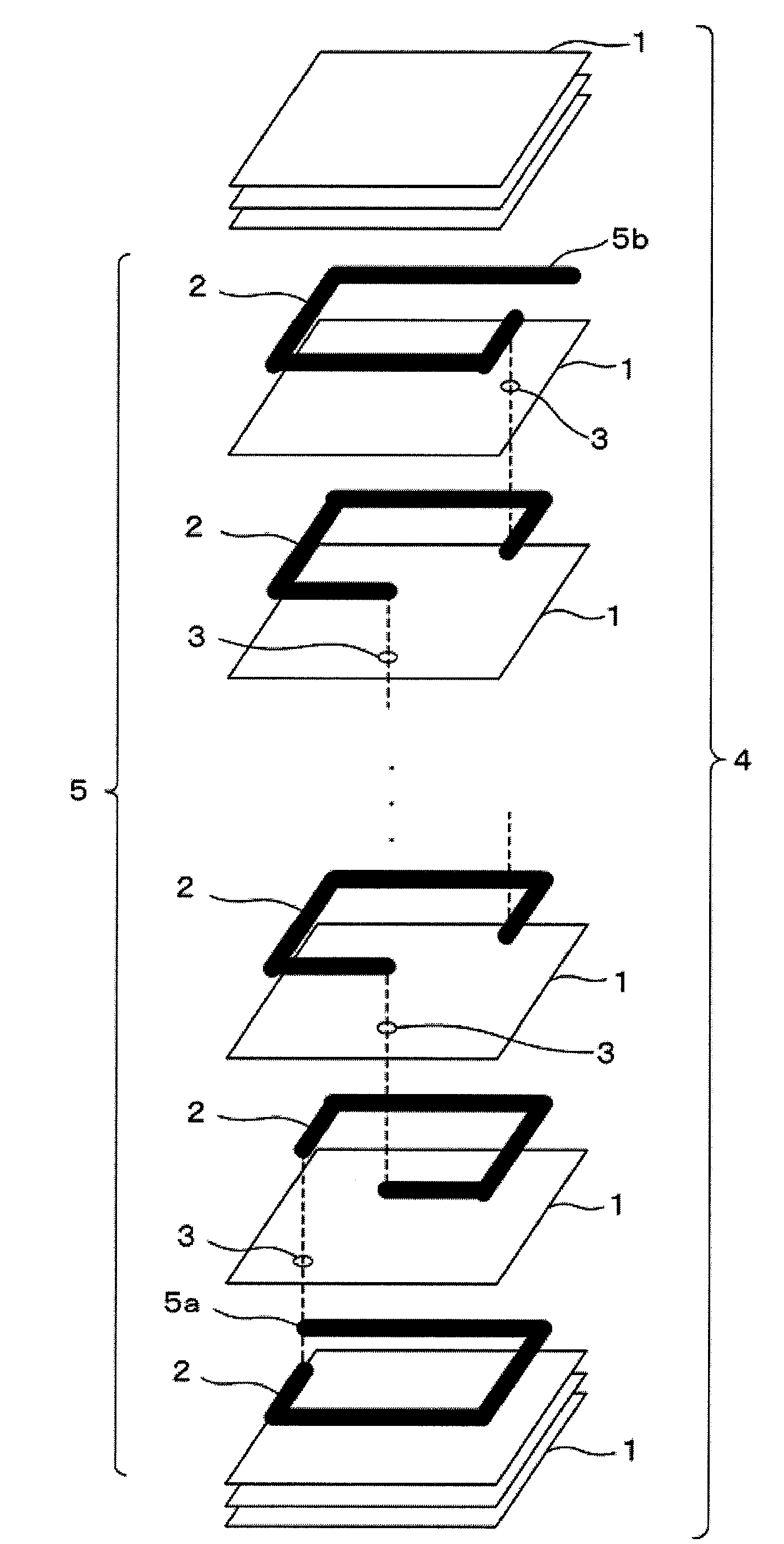
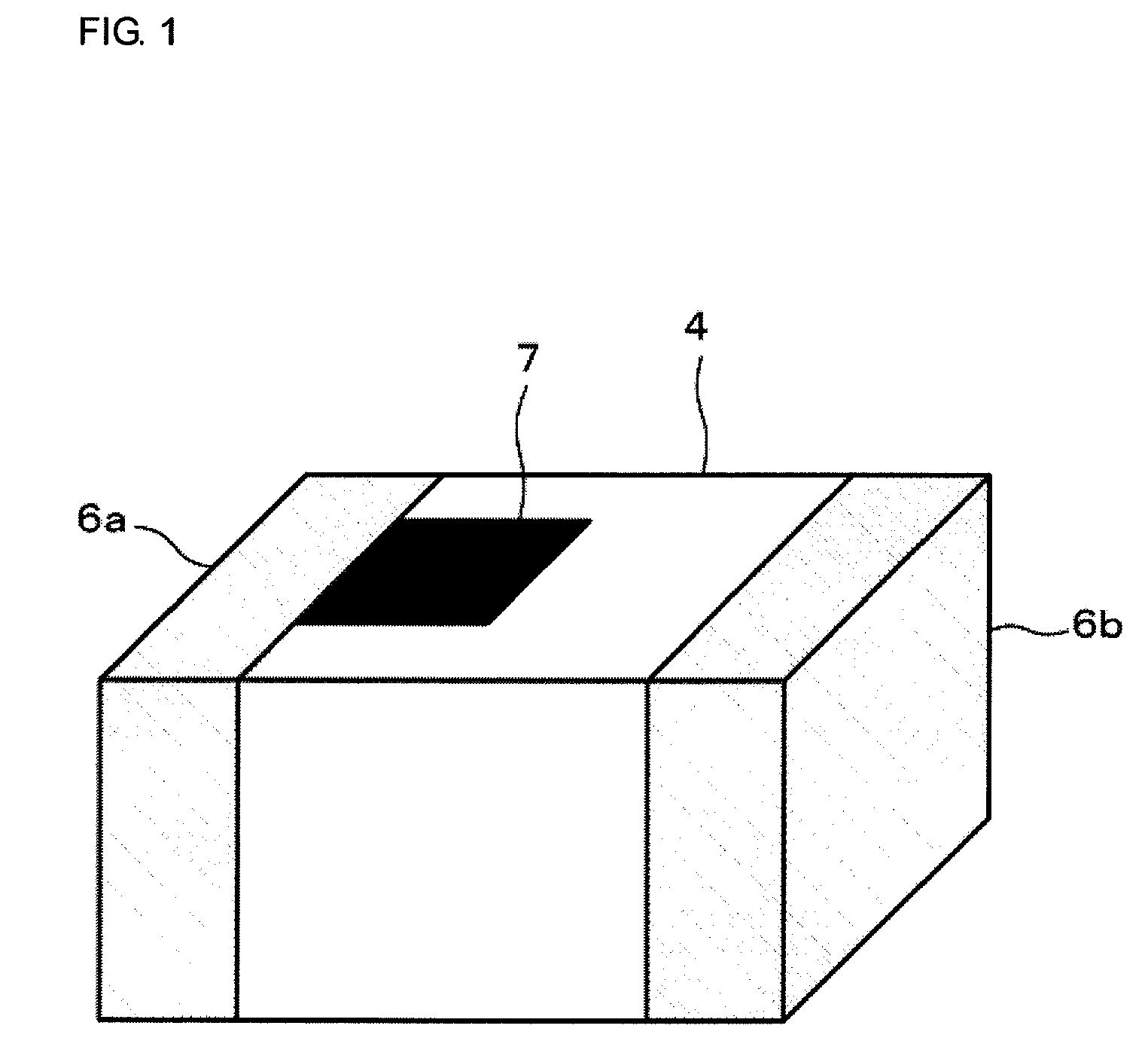
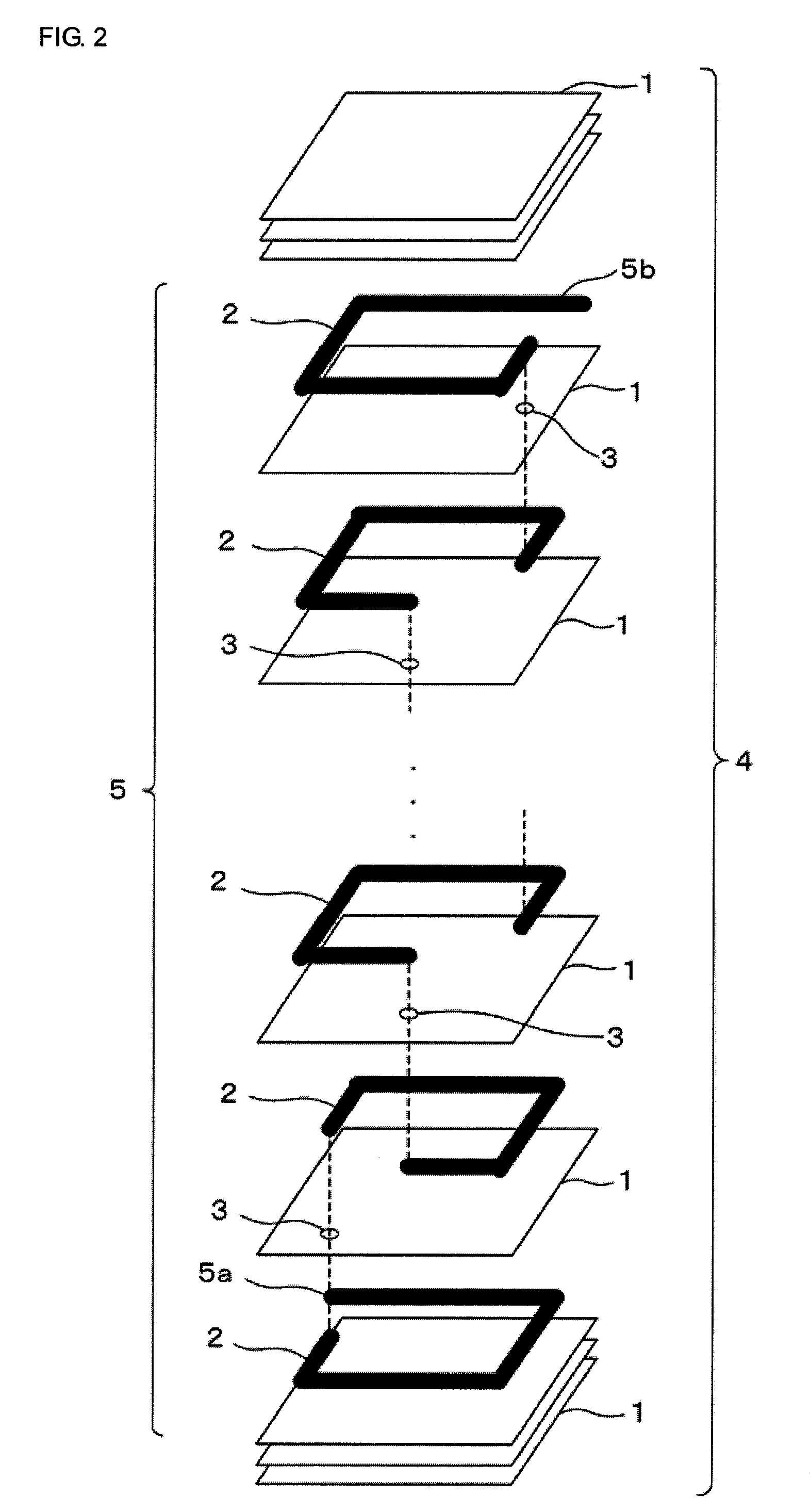
[0102]FIG. 1 is a perspective view showing an external structure of a multilayer wiring chip component (multilayer inductor) according to one embodiment of the present invention, and FIG. 2 is an exploded perspective view showing an internal structure thereof.

[0103]The multilayer wiring chip component of this Example 2 has the structure, as shown in FIGS. 1 and 2, in which conductor layers (internal conductors) 2 containing Ag as a primary component are laminated to each other with glass layers (insulating layers) 1 formed therebetween using the photosensitive glass paste of the present invention, and in which the conductor layers (internal conductors) 2 are connected to each other through via holes 3 (see FIG. 2) to form a spiral coil 5 in a laminate 4.

[0104]External electrodes 6a and 6b (FIG. 1) are provided on two end sides of the ...


PUM

PropertyMeasurementUnit
Temperatureaaaaaaaaaa
Percent by massaaaaaaaaaa

Abstract

A photosensitive glass paste that can be fired at a low temperature for a short period of time and that can suppress generation of voids and diffusion of Ag in glass layers formed by firing, and a high-performance multilayer wiring chip component manufactured by using the above photosensitive glass paste are provided. As a sintering aid glass which is combined with a ceramic aggregate and a primary glass, a glass having a contact angle to the ceramic aggregate smaller than that of the primary glass to the ceramic aggregate is used, and the content of the sintering aid glass is set to 5 to 10 percent by volume of the inorganic component. As the sintering aid glass, a glass containing SiO2, B2O3, CaO, Li2O, and ZnO at a predetermined ratio is preferably used. As the primary glass, a glass containing 70 to 90 percent by weight of SiO2, 15 to 20 percent by weight of B2O3, and 1 to 5 percent by weight of K2O can be used.

Description

[0001]This is a continuation of application Ser. No. PCT / JP2008 / 051292, filed Jan. 29, 2008, the contents of which is hereby incorporated by reference.TECHNICAL FIELD[0002]The present invention relates to a photosensitive glass paste and a multilayer wiring chip component that includes glass layers and conductor layers formed therebetween using a photosensitive Ag paste, the glass layers being formed using the photosensitive glass paste.BACKGROUND ART[0003]As a non-magnetic ceramic material used for manufacturing a ceramic multilayer component having an inductor portion that uses a non-magnetic ceramic including a borosilicate glass, a non-magnetic ceramic that includes a borosilicate glass containing 70 to 90 percent by weight of SiO2, 10 to 30 percent by weight of B2O3, and 5 percent by weight or less of K2O is known (see Patent Document 1).[0004]Since the dielectric constant of a non-magnetic ceramic layer of the inductor portion is extremely low when this non-magnetic ceramic is...

Claims


Application Information

Patent Timeline
IPC IPC(8): H05K1/09C03C3/089
CPCC03C8/02C03C8/04C03C8/14H01F2017/0066G03F7/0047G03F7/029H01F2017/002C03C8/22C03C3/089G03F7/0045H01F17/00
Inventor NISHINO, KOSUKE
Owner MURATA MFG CO LTD
Learn More