Methods for increasing film thickness during the deposition of silicon films using liquid silane materials

a technology of liquid silane and film thickness, which is applied in the field of increasing film thickness during the deposition of silicon films using liquid silane materials, can solve the problems of prohibitively expensive use of conventional cvd techniques to deposit films 1 m, impractical processing of a single substrate at a time, etc., and achieves low cost, simple pre- and post-processing of applied films, and minimizing contamination of resulting films

Inactive Publication Date: 2009-11-19
SILEXOS
View PDF5 Cites 3 Cited by
  • Summary
  • Abstract
  • Description
  • Claims
  • Application Information

AI Technical Summary

Benefits of technology

[0011]Another object of embodiments of the present invention is to be able to apply the film while maintaining uniformity across the substrate, of physical film properties such as thickness, and electrical and optical film properties.
[0012]Still another object of embodiments of the present invention is to allow the inexpensive application of such Si films in a production-based environment.
[0013]Yet another object of embodiments in accordance with the present invention is to apply the films while minimizing contamination of the resulting film from either the ambient atmosphere or materials/equipment that the liquid material may

Problems solved by technology

This makes processing of a single substrate at a time impractical.
Owing to the processing times required to create such thick film

Method used


Image

  • Methods for increasing film thickness during the deposition of silicon films using liquid silane materials
  • Methods for increasing film thickness during the deposition of silicon films using liquid silane materials
  • Methods for increasing film thickness during the deposition of silicon films using liquid silane materials

Examples


example 1

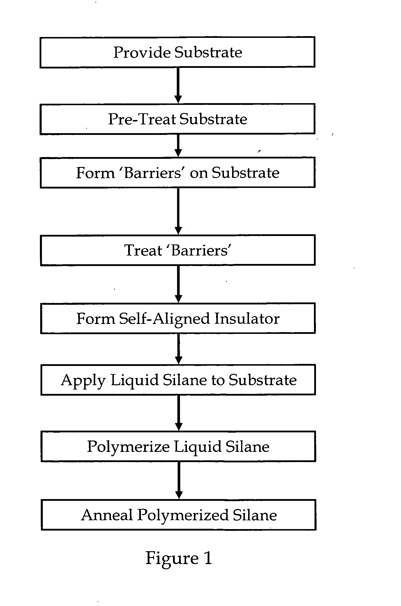
[0101]FIG. 6 shows a simplified flow diagram of an embodiment of a process for forming a silicon layer in accordance with the present invention. Each of the blocks represents a chamber into which the substrate is transferred using a form of conveyor belt from the preceding chamber. Each chamber is interconnected with the adjacent chamber through an interlock (not needed to be hermetic seal) and kept under positive N2 pressure in order to maintain O2 levels at sub 10 ppm in the atmosphere. The O2 environment is needed to protect the films from contamination and adverse changes in the film properties.

[0102]In this particular embodiment, the substrate comprises glass having a thickness of 2-3 mm. Equipment used in the manufacture of flat panel display devices could be applicable to form the silicon layers of the present invention. For example, the tools used in the fabrication of flat panel displays for generation 4 (Glass—730 mm×920 mm) could be used.

[0103]It is understood that the su...

example 2

[0136]FIG. 7 provides an illustration of another example of a process flow illustrating an embodiment of the present invention which implements formation of a silicon film in a manner that optimizes the flow in a production manufacturing environment. Two advantages are offered by this approach. First, it does not require the ink printing of the barrier material. Secondly, it uses electroplating to obtain self aligned barriers. In addition, the Poly Methyl Methacrylate (PMMA) can be replaced by a positively photoresist that might offer the additional advantage of increasing the process time by simply exposing the barrier features using a scanned laser beam. It should be possible to use this approach to create high aspect ratio (i.e. vertical) profile of the barriers.

[0137]1. Prime / Dry

[0138]Again, the substrate is loaded into the chamber. A priming process is applied which prepares the top surface so the PMMA will adhere. Examples of such a priming process include but are not limited ...

example 3

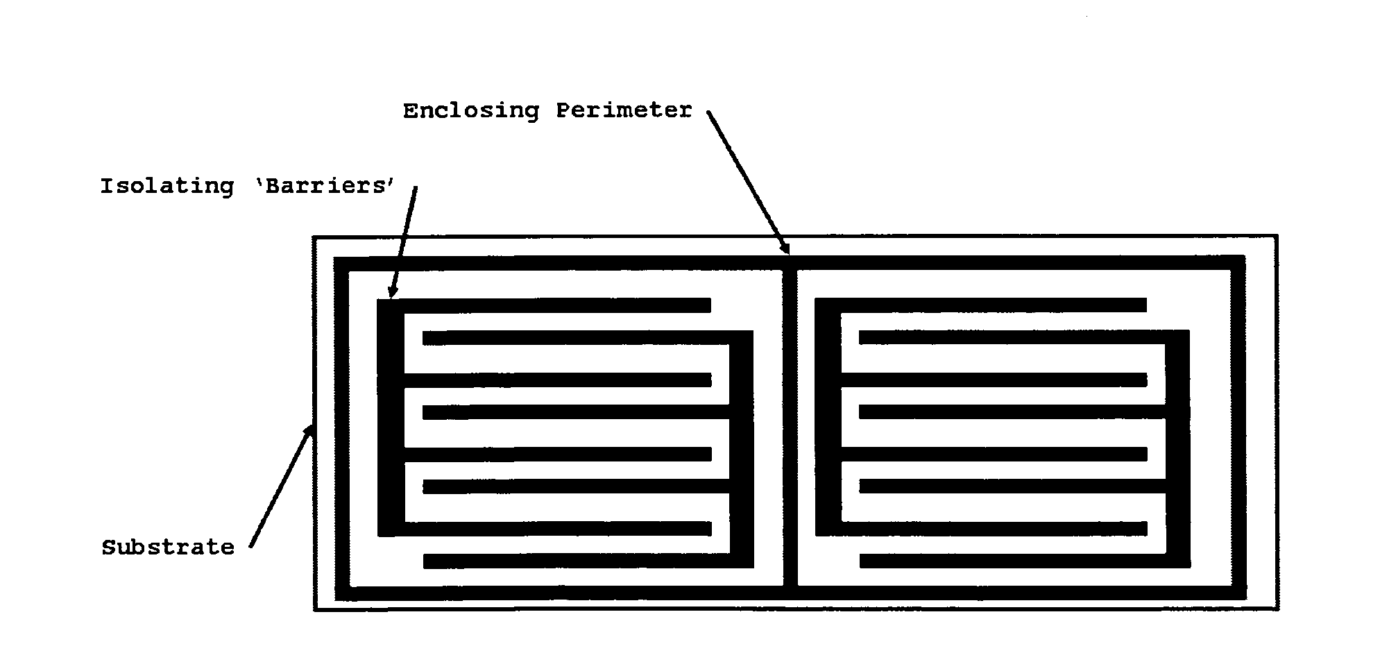
[0169]FIGS. 9A-9C show another method for creating a barrier which can retain the liquid silane fluid during the coating process.

[0170]FIG. 9A shows a top view, and FIG. 9AA shows a side view, depicting how a removable retaining ring can be press fitted against the perimeter of the substrate. If, for example, the substrate is a glass sheet 1.5×1.0 square meters the retaining ring would typically match the outer perimeter in dimensions but have a width approximating 1 centimeter.

[0171]After the retaining ring is pressed against the substrate the liquid silane is dispensed into the ring as shown in FIG. 9B. The liquid fills the cavity formed by the walls of the retaining ring.

[0172]Once the liquid has been dispensed, UV lamps scan the surface of the coated substrate to induce polymerization of the liquid silane into polysilane solid, as shown in the top and side views of FIGS. 9C-9CA. Once the liquid silane has been converted into the solid polysilane, the retaining ring can be remove...


PUM


Abstract

Embodiments in accordance with the present invention relate to the fabrication of thin (>1 μm) polycrystalline, nanocrystalline, or amorphous silicon films on a substrate. Particular embodiments utilize liquid sources of silane, including but not limited to cyclohexasilane (CHS), cyclopentasilane (CPS) or related derivatives of these compounds. In one embodiment, the silane is applied in liquid form contained by the use of a series of raised walls. Subsequent polymerization results in the material being a solid form. In other embodiments, the silane is applied as a liquid which is then frozen, with subsequent localized melting allowing polymerization to convert the material into a stable solid form. Embodiments of the present invention are particularly suited for forming thick (>10 μm) silicon films needed to achieve light absorption efficiencies deemed acceptable for thin film photovoltaic devices.

Description

CROSS-REFERENCE TO RELATED APPLICATION[0001]The instant nonprovisional patent application claims priority to U.S. Provisional Patent Application No. 61 / 054,336 filed May 19, 2008 and which is incorporated by reference in its entirety herein for all purposes.BACKGROUND[0002]Traditional methods for depositing silicon based films, either amorphous, polycrystalline, or crystalline, have relied on using techniques such as Chemical Vapor Deposition CVD, Plasma Enhanced Chemical Vapor Deposition PECVD or Atmospheric Pressure Chemical Vapor Deposition APCVD. A common technique applied in the Integrated Circuit Industry is Low Pressure CVD (LPCVD).[0003]In LPCVD, depending on the particular process, one or more silicon wafers are placed into a vacuum chamber. Gases are evacuated and an inert atmosphere of gas is introduced into the flow while the substrates are heated, often to temperatures of more than 600° C. Silane gas is introduced into the chamber, often in the presence of N2 as an iner...

Claims


Application Information

Patent Timeline
IPC IPC(8): H01L29/04H01L21/20
CPCH01L21/02532H01L21/02573H01L21/02592H01L21/02595H01L21/02623Y02E10/546H01L31/182H01L31/1824H01L31/202Y02E10/545H01L21/02658Y02P70/50
Inventor SIRKIN, ERIC
Owner SILEXOS
Why Eureka
Try Eureka