Organic light-emission device
a technology of organic light-emitting diodes and topemitting oles, which is applied in the direction of organic semiconductor devices, discharge tubes/lamp details, discharge tubes luminescnet screens, etc., can solve the problems of difficulty in injection of holes from the upper transparent electrode, inferior electron injection capability, etc., and achieve high efficiency, high reliability, and prevent the effect of organic layer suffering
- Summary
- Abstract
- Description
- Claims
- Application Information
AI Technical Summary
Benefits of technology
Problems solved by technology
Method used
Image
Examples
example 1
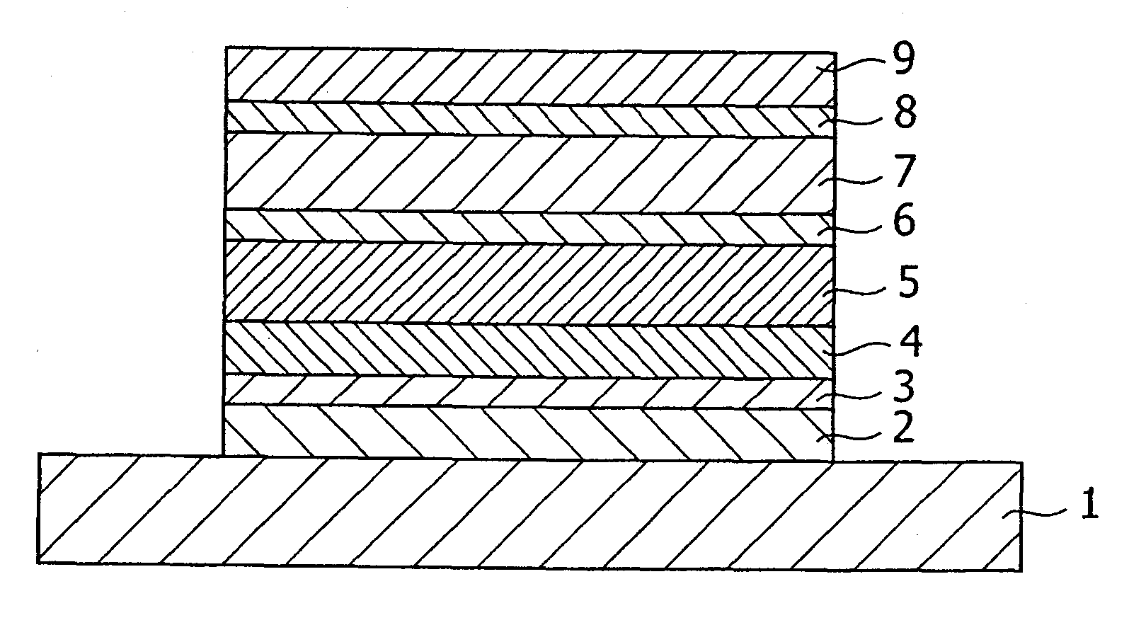
[0039]The FIGURE of drawing is a schematic cross sectional view showing an embodiment of the invention. Mg and Ag were co-deposited as reflective lower cathode 2 at a ratio of 9 / 1 on substrate 1. Li was formed as electron injection layer 3 to a thickness of 1 nm by a resistance heating vapor-deposition method. Electron injection layer 3 was formed in an island form, as opposed to a film form, since the thickness thereof was as small as 1 nm. Tris(8-hydroxyquinoline) aluminum complex was formed as electron transporting layer 4 to a thickness of 10 nm, and then light-emission layer 5 having a thickness of 30 nm (4,4′-bis(2,2′-diphenylvinyl)biphenyl), hole transporting layer 6 having a thickness of 10 nm (4,4′-bis(N-(1-naphthyl)-N-phenylamino)biphenyl) and hole injection layer 7 having a thickness of 20 nm (copper phthalocyanine) were vapor deposited in this order.
[0040]Metallic thin layer 8 was then formed to a thickness of 2 nm by an electron beam vapor deposition method. As a materi...
example 2
[0041]A top-emitting device was produced in the same manner as in Example 1 except that a metallic thin layer having a thickness of 10 nm was formed with Ru (ruthenium). In the resulting device, the metallic thin layer had such a structure that the surface portion thereof in contact with the upper transparent electrode was substantially oxidized, and the ratio of the oxide was gradually decreased in the depth direction, as revealed by XPS. The resulting device exhibited a driving voltage of 8 V and a light-emission efficiency of about 1.5 lm / W, which showed that the structure of the oxidized layer did not adversely affect the hole injection capability.
example 3
[0042]A reflective lower anode (formed of Mg and Ag) was formed on a substrate in an ordinary method. A hole injection layer having a thickness of 20 nm (copper phthalocyanine), a hole transporting layer having a thickness of 10 nm (4,4′-bis(N-(1-naphthyl)-N-phenylamino)biphenyl), a light-emission layer having a thickness of 30 nm (4,4′-bis(2,2′-diphenylvinyl)biphenyl) and electron transporting layer 4 having a thickness of 10 nm (tris(8-hydroxyquinoline) aluminum complex) were formed in this order, and an electron injection layer was formed to a thickness of 1 nm in an island form but not in a film form.
[0043]Metallic thin layer 8 was then formed to a thickness of 2 nm by an electron beam vapor deposition method. As a material for forming the metallic thin layer, V (vanadium) was used. A device having metallic thin layer 8 formed thereon was placed in a DC sputtering apparatus, and an upper transparent anode having a thickness of 100 nm was formed with indium zinc oxide as a target...
PUM
 Abstract
Description
Claims
Application Information

