Test probe

a test probe and probe body technology, applied in the field of test probes, can solve the problems of affecting the manufacture cost, not being carried out by a batch fabrication, and not being able to meet the requirements of testing, so as to improve the no-clean property, reduce the contact force, and improve the effect of no-clean property

Inactive Publication Date: 2009-11-26
IPWORKS TECH CORP
View PDF2 Cites 6 Cited by
  • Summary
  • Abstract
  • Description
  • Claims
  • Application Information

AI Technical Summary

Benefits of technology

[0009]A primary object of the present invention is to provide a test probe, which can stabilize the test quality of wafer probing test, and prevent the probe tip of the test probe from being wetted with a to-be-tested die, so as to lower the cleaning frequency of the test probe, increase the utility rate of test machines, and increase the test yield of the die for the purpose of reducing the entire test cost. The test probe of the present invention is coated with a nano-film of conducting polymer, so that the test probe made of Be—Cu alloy can provide the same electro-conductivity as a traditional test probe by only plating a gold layer of one fifth of original thickness. Thus, the cost of whole probe material can be reduced.
[0014]The present invention is related to a test probe which has a probe surface coated with a nano-film of conducting polymer, so that the test probe can efficiently provide better no-clean property, stabler electro-conductivity, lower contact force, and longer usage lifetime.
[0015]The present invention is related to a test probe which is used to stabilize the test quality, wherein the test probe is designed according to the principle of approximately no attraction between the test probe and a to-be-tested die (or an integrated circuit (IC) component), so as to provide better no-clean property. Thus, the present invention can lower the cleaning frequency of the test probe, increase the utility rate of test machines, increase the test yield of the die, and reduce the entire test cost.

Problems solved by technology

Thus, a wafer probing test is one of important processes in the integrated circuit fabrication, which affects the manufacture cost thereof.
However, the fixing operation may cost much labor power and time, and can not be carried out by a batch fabrication manner, so that the manufacture cost of the test fixture can not be efficiently lowered.
The foregoing complicated processes cause that the usage lifetime of the test probes on the test fixture becomes one of factors affecting the manufacture cost of the test fixture.
In other words, it is difficult to maintain sufficient yield and stability if a plurality of to-be-tested dies or integrated circuit (IC) components are simultaneously tested.
However, after the test probes are repeatedly penetrated into the pad surface of several to-be-tested dies, the probe tip of the test probes may be easily wetted with solder, resulting in deteriorating the test quality or causing erroneous test.
As a result, the test yield may be rapidly lowered.
Although the overdrive contact force can be used to solve the foregoing problem and enhance the test yield, the overdrive contact force may damage other lower structure under the pad surface of the to-be-tested dies.
However, once the number of the test probes is increased or the pitch between the adjacent test probes is decreased, the cleaning frequency of the test probes may be considerably increased, resulting in lowering the utility rate of test machines and shortening the lifetime of the test probes.
To increase the electro-conductivity of the test probes, the Be—Cu surface of the test probes will be coated with a gold (Au) layer which generally has a thickness about 2-100 μm, resulting in increasing the whole cost of the test probes.
In addition, there is a wetting problem generally existing in the test probes.
Especially, when a leadless solder process is used, the wetting problem will be worse than that of traditional lead-containing solder process.
Furthermore, when the test is carried out under high temperature, the wetting problem will be worse than that of the test under room temperature.
Recently, although related manufacturers develop a kind of test probe having a surface coated with a metal film to elongate the lifetime of the test probe, the wetted problem still cannot be solved.
Moreover, the metal film cannot maintain identical resistance value when the test probe is used to test.
As a result, the metal film still cannot enhance the test yield and the test stability.

Method used


Image

  • Test probe
  • Test probe

Examples


Embodiment Construction

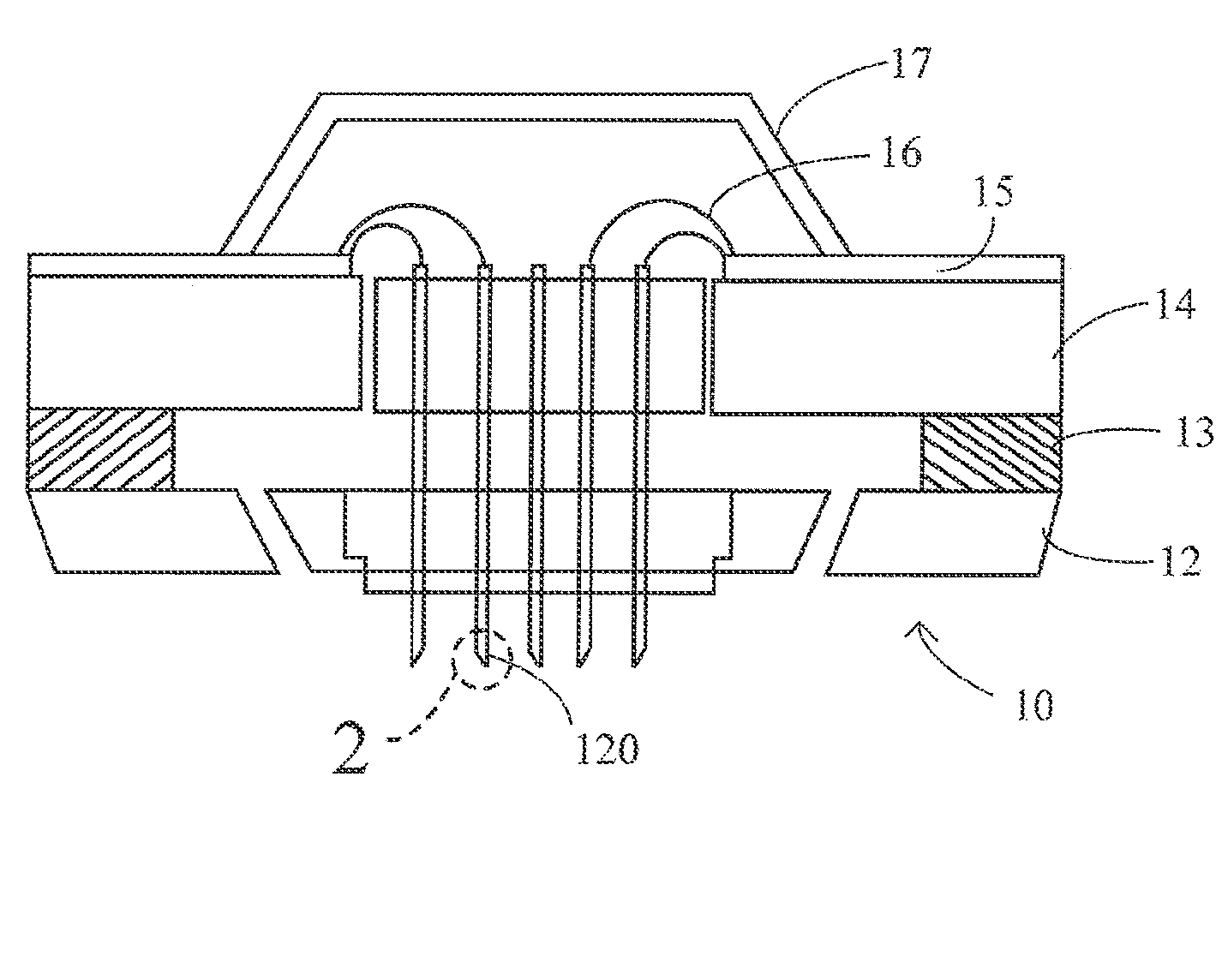
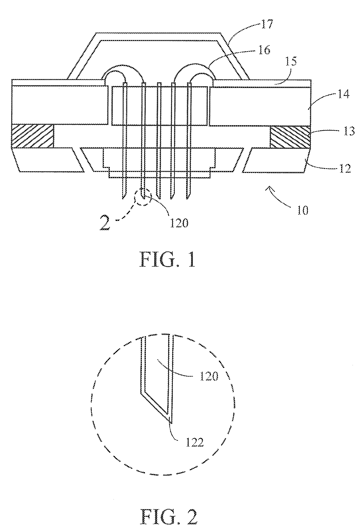
[0019]A preferred embodiment of the present invention provides a test probe which comprises a plurality of probes and a nano-film of conducting polymer, wherein the probes are made of metal material and installed on a test fixture, and the nano-film of conducting polymer is coated on the probes.

[0020]In the present invention, the nano-film of conducting polymer can be preferably selected from conducting polymer having a no-clean property. For example, the conducting polymer can be selected from the group consisting of polypyrrole, polyparaphenylene, polythiophene, polyaniline, combination thereof, and derivative thereof. The thickness of the nano-film of conducting polymer is preferably about 1-20 nanometer (nm), especially about 1-5 nm.

[0021]In the present invention, the probes are made of the metal material which can be preferably selected from the group consisting of nickel (Ni), gold (Au), copper (Cu), tungsten (W), rhenium (Re), titanium (Ti), beryllium (Be), stainless steel, o...


PUM


Abstract

A test probe pin is disclosed. The test probe has a plurality of probes, each of which has a probe tip surface coated with a nano-film of conducting polymer, and the thickness of the nano-film is about 1-20 nm. The probes coated with the nano-film are installed on a test fixture for testing IC components, so that the probes can efficiently provide excellent no-clean property and stabler electro-conductivity for lowering the cleaning frequency of the probes, enhancing the yield of IC component testing, increasing the utility rate of the test fixture, reducing the total testing cost, elongating the usage lifetime of the test probe, and reducing the cost of probe material. Thus, due to the nano-film of conducting polymer, the probes made of metal material can provide almost the same electro-conductivity as a traditional probe by only plating a gold layer of one fifth of original thickness, so that the cost of whole probe material can be reduced.

Description

FIELD OF THE INVENTION[0001]The present invention relates to a test probe of a test fixture for integrated circuit (IC) components probing, and more particularly to a test probe coated with a nano-film of conducting polymer material.BACKGROUND OF THE INVENTION[0002]Traditional test probes applied to a test fixture are mainly made of beryllium-copper (Be—Cu) alloy and has a surface coated with a gold (Au) layer. The size and shape of the test probes may be varied according to-be-tested integrated circuit (IC) components, but the basic structure thereof is the same and comprises probe pins, sleeves, and springs. The test probes of the test fixture can be applied to various fields, such as test probes for printed circuit board (bare board and finished board), test probes for semiconductor test, test probes for display panel, and test probes for components of telecommunication products including various connectors for antennae of mobile phones, batteries, loudspeakers, vibrators, LCD pa...

Claims


Application Information

Patent Timeline
Patent Type & Authority Applications(United States)
IPC IPC(8): G01R31/02G01R1/067
CPCG01R1/07314G01R1/06761
Inventor CHEN, BEEN-LONGCHEN, HUANG-CHIH
Owner IPWORKS TECH CORP
Why Eureka
Try Eureka