Method for Manufacturing Semiconductor Apparatus Having Saddle-Fin Transistor and Semiconductor Apparatus Fabricated Thereby

a manufacturing method and technology of semiconductor devices, applied in the direction of semiconductor devices, electrical devices, basic electric elements, etc., can solve problems such as degrading the reliability of operation, and achieve the effects of improving the short channel effect and the current driving capacity of the transistor, reducing mis-arrangement, and improving the uniformity of transistor characteristics

Active Publication Date: 2009-12-03
SK HYNIX INC
View PDF5 Cites 28 Cited by
  • Summary
  • Abstract
  • Description
  • Claims
  • Application Information

AI Technical Summary

Benefits of technology

[0031]The saddle-fin transistor formed as a cell transistor may reduce mis-arrangement between a gate electrode and a fin region. The multi-channel fin transistor having a three-dimensional channel formed in the core region and the peripheral region may improve a short channel effect and a current driving capacity of the transistor in all regions of the semiconductor memory apparatus.
[0032]The saddle-fin transistor as a cell transistor formed to have a three-dimensional channel structure instead of a plane channel structure in the core region and the peripheral region may improve uniformity of characteristics of the transistor.
[0033]In one embodiment, a gate mask pattern may include a gate mask pattern for forming a gate structure of the cell transistor and a gate mask pattern for forming a gate structure of the transistor in the core region and the peripheral region. Using one gate mask pattern, the mis-arrangement between gate patterns of the transistor included in the core region and the peripheral region can be reduced, and operation defects and characteristic degradation of the semiconductor memory apparatus can be prevented.

Problems solved by technology

Moreover, the junction resistance is increased by reduction of the junction area to reduce a driving current of the transistor, thereby degrading the reliability of the operation.

Method used


Image

  • Method for Manufacturing Semiconductor Apparatus Having Saddle-Fin Transistor and Semiconductor Apparatus Fabricated Thereby
  • Method for Manufacturing Semiconductor Apparatus Having Saddle-Fin Transistor and Semiconductor Apparatus Fabricated Thereby
  • Method for Manufacturing Semiconductor Apparatus Having Saddle-Fin Transistor and Semiconductor Apparatus Fabricated Thereby

Examples


Embodiment Construction

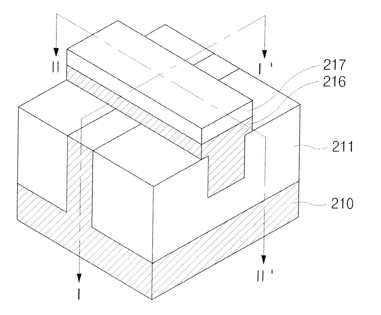
[0038]FIGS. 1 to 2f illustrate a process for fabricating a saddle-fin transistor having a three-dimensional channel structure that is used as a cell transistor.

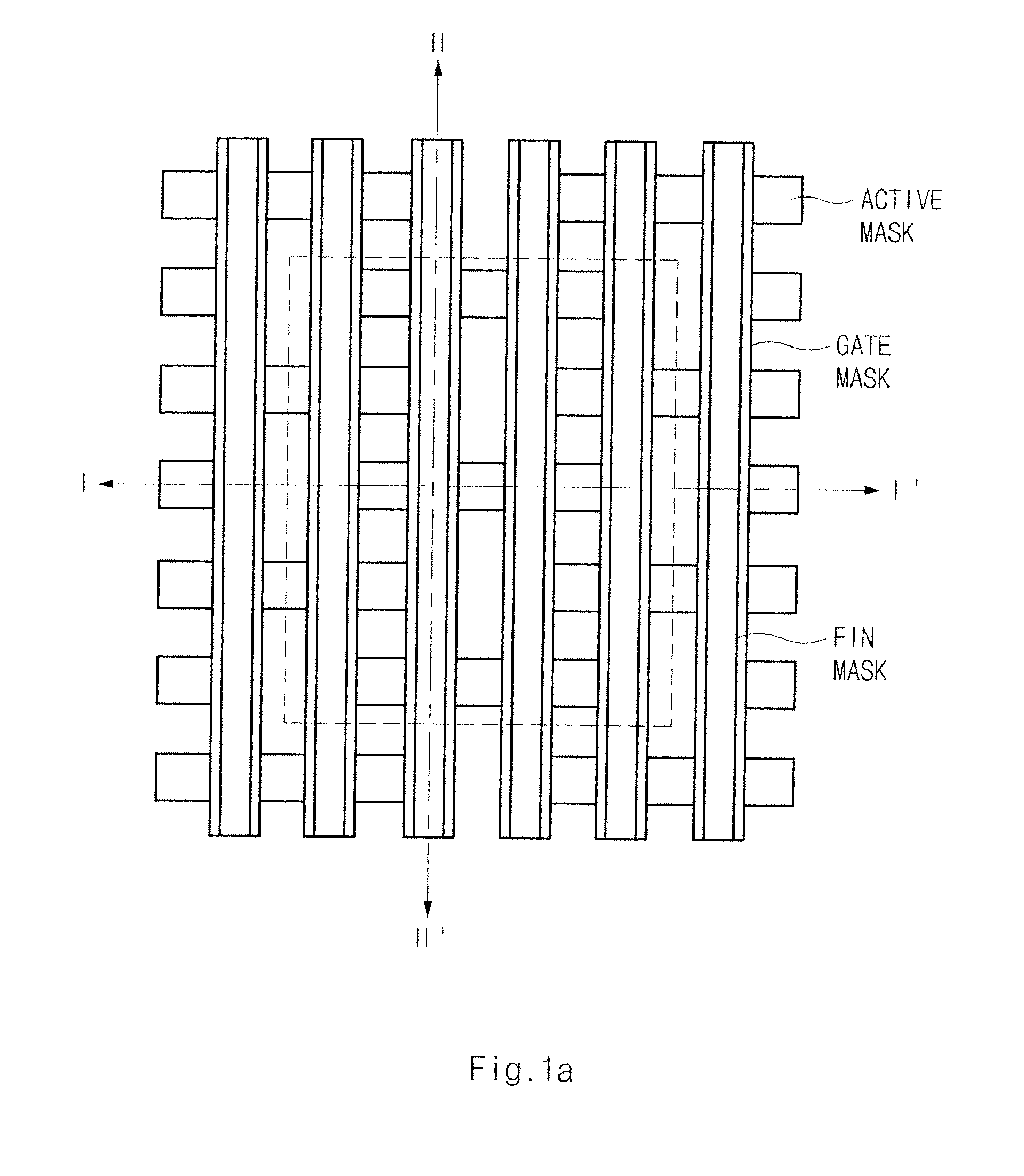
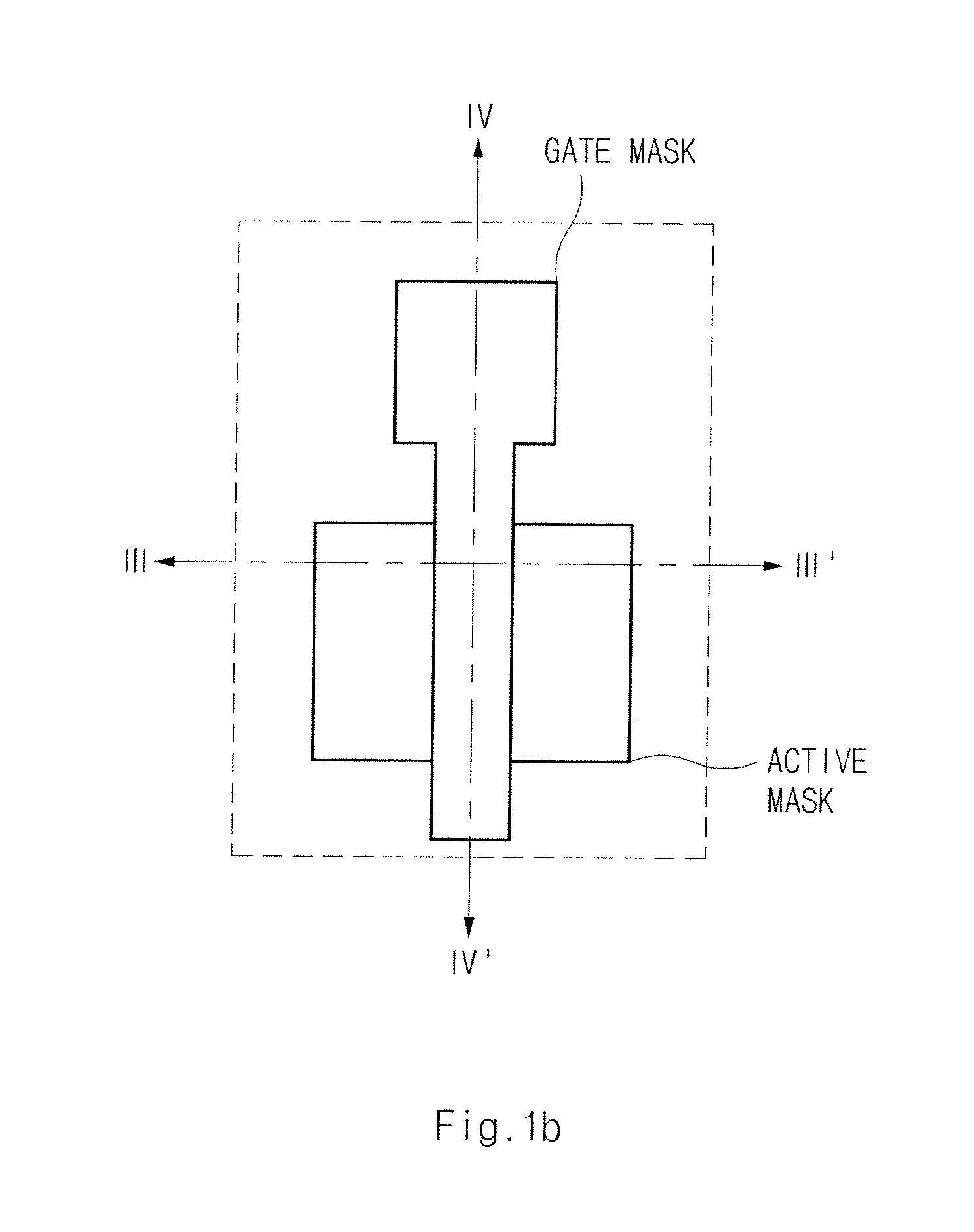
[0039]FIG. 1a and 1b are plane diagrams illustrating a mask pattern for fabricating a saddle-fin transistor of a semiconductor apparatus according to an embodiment of the present invention.

[0040]Referring to FIG. 1a, active masks are arranged in a horizontal direction (I-I′), and a gate mask and a fin mask are arranged in a vertical direction (II-II′). The active masks, the gate mask, and the fin mask shown in FIG. 1a are used for manufacturing a saddle-fin transistor as a cell transistor included in each unit cell of the semiconductor memory apparatus.

[0041]Referring to FIG. 1b, active masks are arranged in a horizontal direction (III-III′), and gate masks are arranged in a vertical direction (IV-IV′), for manufacturing a transistor included in the core region and the peripheral region. The transistor, which is manufactured ...


PUM


Abstract

A method for manufacturing a semiconductor memory apparatus may include forming a channel region and a gate region through a self-alignment etching process on a cell region; and forming a three-dimensional multi-channel region through an etching process using a first multi-channel mask on a core region and a peripheral region and forming a gate region through an etching process using a second multi-channel mask, thereby preventing mis-arrangement of gates.

Description

CROSS-REFERENCES TO RELATED APPLICATIONS[0001]Priority is claimed to Korean patent application number 10-2008-0050942, filed on May 30, 2008, which is incorporated by reference in its entirety.BACKGROUND OF THE INVENTION[0002]The present invention generally relates to a method for manufacturing a high-integrated semiconductor apparatus, and more specifically, to a method for manufacturing a semiconductor apparatus with plural transistors such as a saddle-fin transistor and a multi-channel transistor.[0003]A dynamic random access memory (DRAM) as a representative example of semiconductor apparatus includes a plurality of unit cells each including a capacitor and a transistor. A capacitor is used to temporarily store data, and a transistor is used to transmit data between a bit line and the capacitor in response to a control signal (word line) using a semiconductor property that is the electric conductivity changing depending on environment. The transistor includes a gate, a source an...

Claims


Application Information

Patent Timeline
Patent Type & Authority Applications(United States)
IPC IPC(8): H01L29/78H01L21/336
CPCH01L27/10876H01L27/10879H01L29/785H01L29/66795H01L27/10894H10B12/056H10B12/053H10B12/09H10B12/36
Inventor LEE, SANG DON
Owner SK HYNIX INC
Why Eureka
Try Eureka