Planar optical waveguide array module and method of fabricating the same

Inactive Publication Date: 2009-12-03
HITACHI LTD
4 Cites 7 Cited by

AI-Extracted Technical Summary

Problems solved by technology

As communication systems grow larger in capacity making it necessary for each device to process data at a rate of Tbits/s or higher, severer problems will be posed, for example, concerning the number of electrical transmission lines to be used and crosstalk between lines.
Using electrical transmission lines for such high-speed, large-volume signal transmission will make problems such as transmission delays and noise more conspicuous.
In such a case, the positioning margins for accurately positioning different optical parts on the same substrate are small, so that it is d...

Benefits of technology

[0017]According to the fabrication method of the present invention, with the optical element array driven by a bias applied thereto, the optical waveguide array is brought near the optical element array, and the optical axes of the optical waveguide array and the optical element array are aligned while monitoring output signals outputted from the outermost optical waveguide channels on both sides of the optical waveguide array or from the outermost optical element channels on both sides of the optical element array. This method makes it possible to optically connect a film optical waveguide array and an optical element array highly efficiently and stably.
[0018]Each of the outermost optical waveguide channels on both sides of the optical waveguide array is provided with a mirror structure for light redirection. This makes it possible to monitor from above the optical signals which are received from optical elements (i.e. laser elements in the present example) optically connected to the optical waveguide array and then transmitted through the outermost optical waveguide channels extending along the horizontal substrate surface. Therefore, optical waveguides can be connected to optical connectors, or optical waveguides supported by a jig can be mounted on a board with ease while monitoring the optical signals.
[0019]The present invention also provides a planar optical waveguide array module in which a flexible printed circuit board having electrical wirings is formed on the surface of an optical waveguide array and in which surface illuminated type photodiodes for optical signal monitoring are mounted on the surface of the flexible printed circuit board, each to be directly above a mirror structure for light redirection. In this configura...

Abstract

The optical element array and an optical waveguide array are optically connected on the substrate. The optical waveguide array includes optical waveguide channels which are the outermost optical waveguide channels on both sides of optical waveguide array channels and each of which is provided with a mirror structure for light redirection. With the optical element array driven by a bias applied thereto, the optical waveguide array is brought near the optical element array. The optical axes of the optical waveguide array channels and the optical element array are aligned while monitoring optical signals outputted from the outermost optical waveguide channels on both sides of the optical waveguide array channels via the mirror structures for light redirection. The optical waveguide array is fixed to the substrate in such a position that the optical signals have a desired output value.

Application Domain

Optical articlesCoupling light guides +2

Technology Topic

Waveguide channelPlanar optical waveguide +5

Image

  • Planar optical waveguide array module and method of fabricating the same
  • Planar optical waveguide array module and method of fabricating the same
  • Planar optical waveguide array module and method of fabricating the same

Examples

  • Experimental program(7)

Example

Embodiment 1
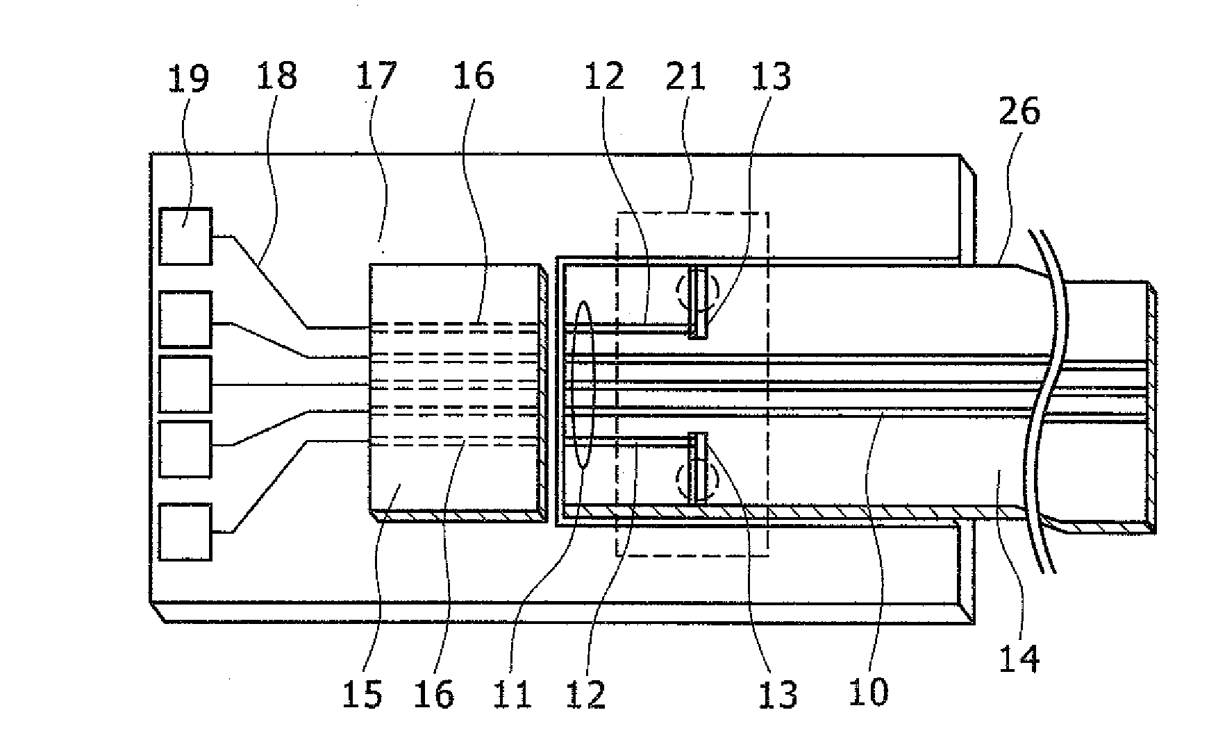
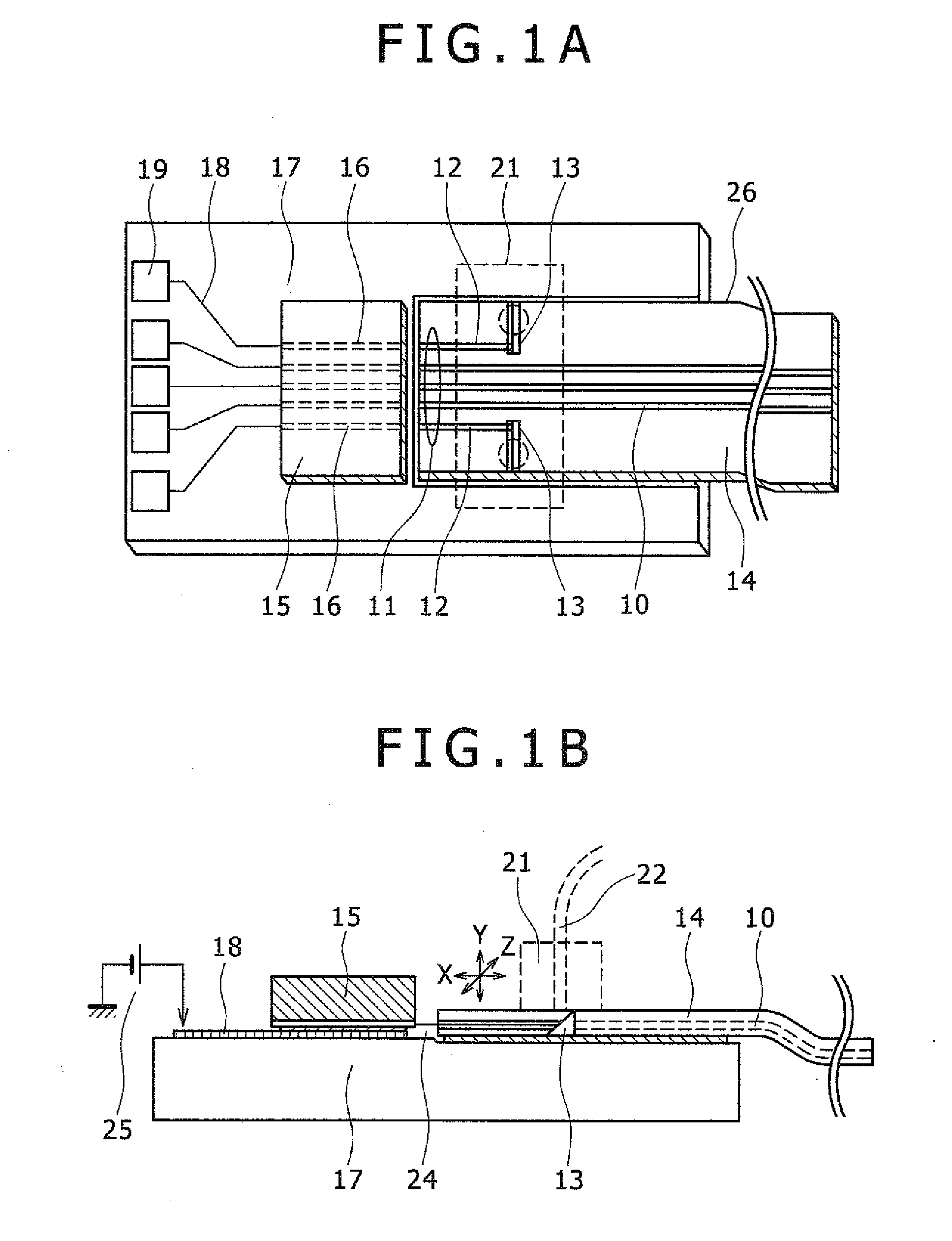
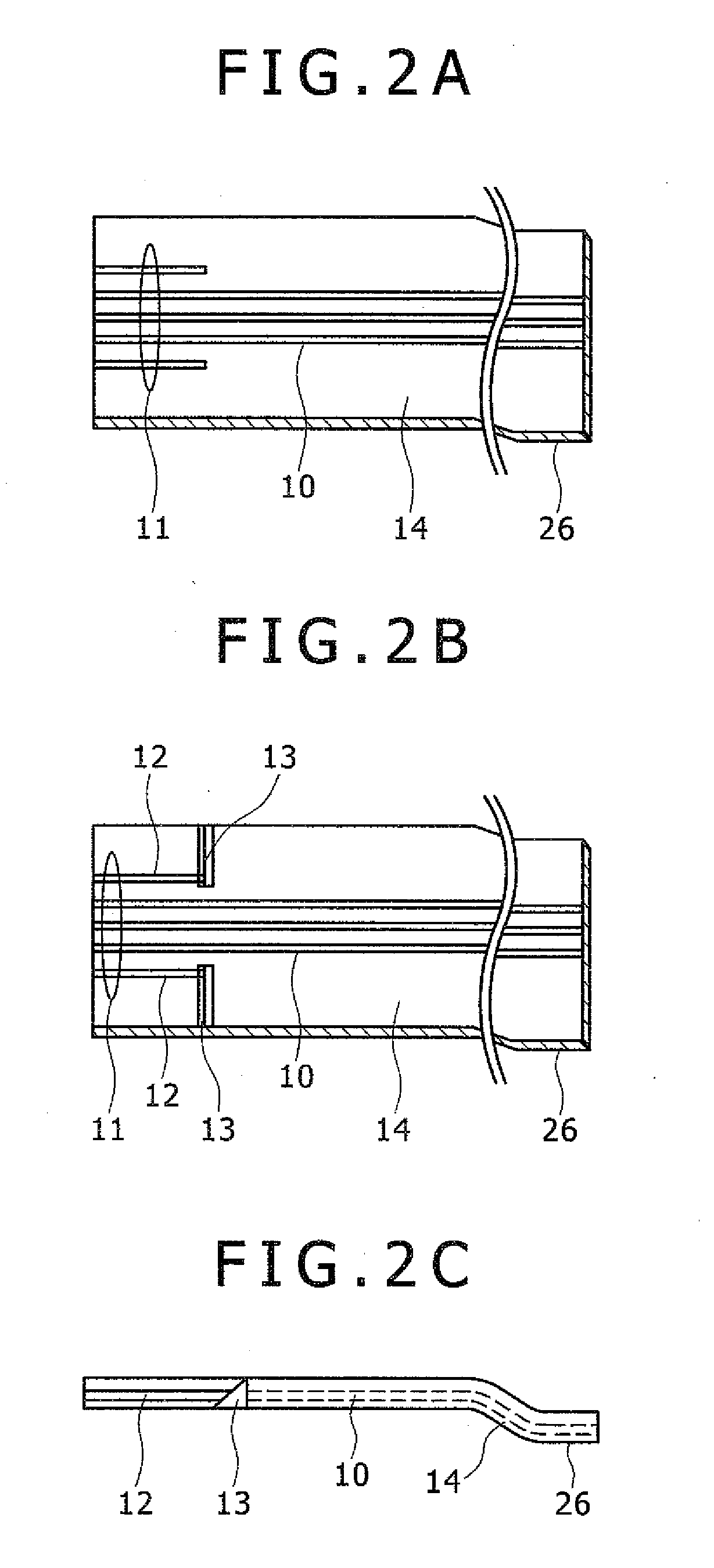
[0042]FIGS. 1A and 1B are a plan view and a sectional view, respectively, of a planar optical waveguide array module according to a first embodiment of the present invention. An optical element array 15 is disposed on a substrate 17. The optical element array 15 and an optical waveguide array 26 are optically connected on the substrate 17. The optical waveguide array 26 includes optical waveguide channels 12 which are the outermost ones on both sides of optical waveguide array channels 11 and each of which is provided with a mirror structure for light redirection 13. The planar optical waveguide array module is fabricated through steps outlined as follows: with the optical element array 15 driven by a bias 25 applied thereto, the optical waveguide array 26 is brought near the optical element array 15; the optical axes of the optical waveguide array channels 11 and the optical element array 15 are aligned while monitoring optical signals 24 outputted from the outermost optical waveguide channels 12 on both sides of the optical waveguide array channels 11 via the mirror structures for light redirection 13; and the optical waveguide array 26 is fixed to the substrate 17 in such a position that the optical signals 24 have a desired output value.
[0043]With reference to FIGS. 2A to 2I, the procedure for fabricating the planar optical waveguide array module according to the first embodiment of the present invention will be described in detail.
[0044]FIG. 2A shows the optical waveguide array 26 which is an optical wiring portion of the planar optical waveguide array module according to the present embodiment. First, the optical waveguide array 26 is fabricated. The optical waveguide array 26 has, as shown in FIG. 2A, the optical waveguide array channels 11 including at least two wiring cores 10 (optical waveguide channels). The wiring cores 10 are enclosed in a cladding layer 14 and formed of a material with a refractive index higher than that of the cladding layer 14. The material of which the optical waveguide array 26 is formed is required to be one, for example, a polymer resin, which is transparent for the light of the optical wavelength to be used and which is flexible to be bendable with a required curvature.
[0045]Next, as shown in FIGS. 2B and 2C, each of the outermost optical waveguide channels 12 on both sides of the optical waveguide array channels 11 is provided with the mirror structure 13 for redirecting light transmitted in the optical waveguide extending in a direction parallel with the horizontal substrate surface into a direction perpendicular to the horizontal substrate surface. The mirror structure 13 for light redirection may be formed in an optional way. It may be formed, for example, by dice cutting, laser irradiation, lithographic patterning, or by mounting a separately prepared mirror part directly to the optical waveguide. The mirror inclination angle is preferably about 45 degrees so that the light transmitted in a direction parallel with the horizontal substrate surface can be redirected by 90 degrees.
[0046]FIG. 2D is a plan view of the optical waveguide array 26 with a positioning guide hole 30 formed outside each of the outermost optical waveguide channels 12 on both sides of the optical waveguide array channels 11. Installing an optical fiber connector having a guide pin structure being described later in the guide holes 30 enables optical axis alignment between the optical waveguide array channels 11 and the optical element channels. The guide holes 30 may be formed by any appropriate method, for example, by etching, drilling, or using laser.
[0047]FIG. 2E is a diagram showing a manner in which the optical element array 15 is mounted on the substrate 17. The substrate 17 is a semiconductor, for example, ceramic or silicon. An electrical wiring 18 and a solder pattern 31 for soldering the optical element array 15 are formed on the surface of the substrate 17. To mount the optical element array 15, the solder pattern 31 is heat-melted with the optical element array 15 held in close contact with the solder pattern 31. The optical element array 15 includes edge emitting laser diodes for a transmitter module or edge illuminated type photodiodes for a receiver module.
[0048]Next, as shown in FIGS. 2F and 2G, an optical fiber connector 21 having a guide pin structure is fitted to the guide holes formed in the optical waveguide array 26, and the optical waveguide array 26 is brought near the substrate 17 on which the optical element array 15 is mounted. Then, with the optical element array 15 (including laser elements in the present example) driven (emitting light) by the bias 25 applied thereto via electrode pads 19 and the electrical wiring 18, optical signals transmitted through the outermost optical element channels 16 on both sides of the optical element array 15 are inputted to optical fibers 22 via the outermost optical waveguide channels 12 on both sides of the optical waveguide array channels 11 and the mirror structures 13 for light redirection. Subsequently, the optical axes of the optical waveguide array 26 and the optical element array 15 are aligned by moving the optical waveguide array 26 in X, Y, and Z directions. This is done while monitoring the optical signals inputted to the optical fibers. The optical waveguide array 26 is fixed to the substrate 17 in such a position that the optical signals each have a desired output value.
[0049]FIGS. 2H and 2I are diagrams showing a planar optical waveguide array module fabricated by the fabrication method described above with reference to FIGS. 2A to 2G. The optical connector 21 is removed from the optical waveguide array 26 after, as described with reference to FIGS. 2F and 2G, the optical axes of the optical element array 15 and optical waveguide array 26 are aligned and the optical waveguide array 26 is fixed to the substrate 17. The optical waveguide array 26 is fixed to the substrate 17 using, for example, an adhesive 33.

Example

Embodiment 2
[0050]FIGS. 3A and 3B are a plan view and a sectional view, respectively, of a planar optical waveguide array module, including a surface light-emitting diode array, according to a second embodiment of the present invention. In this embodiment, a laser element array 40 mounted on a substrate 17 is a surface light-emitting diode array which emits light in a vertical direction to the element surface. To fabricate the planar optical waveguide array module according to the second embodiment, an optical waveguide array 26 is brought near the laser element array 40. The optical waveguide array 26 includes, in addition to a first mirror structure 13 for light redirection provided for each of the outermost optical waveguide channels 12 on both sides of optical waveguide array channels, a second mirror structure 42 formed in an end portion thereof. The subsequent fabrication steps are similar to those described with reference to FIGS. 2A to 2F. Namely, with the surface light-emitting diode array 40 driven by a bias 25 applied thereto via electrode pads 19 and electrical wirings 18, optical signals transmitted through the optical element channels 16, i.e. the outermost optical element channels on both sides of the surface light-emitting diode array 40 are, after being redirected by the second mirror structure 42, inputted to optical fibers 22 via the optical waveguide channels 12, i.e. the outermost ones on both sides of the optical waveguide array channels and the first mirror structures 13. The optical axes of the optical waveguide array 26 and the surface light-emitting diode array 40 are then aligned by moving the optical waveguide array 26 in X, Y, and Z directions. This is done while monitoring the optical signals inputted to the optical fibers. The optical waveguide array 26 is fixed to a support member 41 on the substrate 17 in such a position that the optical signals 24 have a desired value. The support member 41 disposed between the optical waveguide array 26 and the substrate 17 has a thickness which causes the distance between the surface light-emitting diode array 40 and the optical waveguide array 26 to be as desired. The support member 41 is made of a material with a thermal expansion coefficient equal to or intermediate between those of the optical waveguide array 26 and the substrate 17. Using such a material is effective in preventing the optical waveguide array 26 and the substrate 17 from being shifted relative to each other due to thermal expansion caused when they are fixed together.

Example

Embodiment 3
[0051]FIG. 4 is a sectional view of a planar optical waveguide array module, including an edge illuminated type photodiode array, according to a third embodiment of the present invention. To fabricate the planar optical waveguide array module according to the third embodiment, an edge illuminated type photodiode array 50 is driven by applying a bias 25 (i.e. a reverse bias in this case) thereto via electrode pads 19 and electrical wirings 18. With the edge illuminated type photodiode array 50 thus driven, optical signals 24 outputted from optical fibers 22 are inputted to the outermost optical element channels on both sides of the edge illuminated type photodiode array 50 via the mirrors 13 for light redirection and the outermost optical waveguide channels on both sides of optical waveguide array channels. The optical axes of the edge illuminated type photodiode array 50 and the optical waveguide array 26 are then aligned while monitoring electrical signals 51 outputted, after photoelectrical conversion, from the optical element channels. The optical waveguide array 26 is fixed to a substrate 17 in such a position that the electrical signals 51 have a desired value.

PUM

no PUM

Description & Claims & Application Information

We can also present the details of the Description, Claims and Application information to help users get a comprehensive understanding of the technical details of the patent, such as background art, summary of invention, brief description of drawings, description of embodiments, and other original content. On the other hand, users can also determine the specific scope of protection of the technology through the list of claims; as well as understand the changes in the life cycle of the technology with the presentation of the patent timeline. Login to view more.

Similar technology patents

Method of fabricating a dual gate oxide

InactiveUS20050170575A1simplifies fabricationcost reduction
Owner:SAMSUNG ELECTRONICS CO LTD

Apparatus and method of fabricating emitter using arc

InactiveUS20060181220A1simplifies fabrication
Owner:SAMSUNG ELECTRONICS CO LTD

Double-sided electrodynamic screen films

ActiveUS20200061678A1simplifies fabricationcost reduction
Owner:EASTMAN KODAK CO

Liquid crystal panel and fabricating method thereof

ActiveUS20170322448A1simplifies fabricationcost saving
Owner:WUHAN CHINA STAR OPTOELECTRONICS TECH CO LTD

Classification and recommendation of technical efficacy words

  • simplifies fabrication

Intergrated photonic crystal structure and method of producing same

InactiveUS20040264903A1simplifies fabricationneed of be complex
Owner:IGNIS PHOTONYX

Steel sheet with high mechanical strength, ductility and formability properties, production method and use of such sheets

ActiveUS20140170439A1reduce fabrication costsimplifies fabrication
Owner:ARCELORMITTAL INVESTIGACION Y DESARROLLO SL

Patterned printing plates and processes for printing electrical elements

ActiveUS20080092377A1simplifies fabricationless wasteful
Owner:MOLEX INC

Metal-insulator-metal capacitor and fabrication method thereof

ActiveUS20080191311A1simplifies fabricationcost reduction
Owner:SEMICON MFG INT (SHANGHAI) CORP

Method of fabricating flash memory

InactiveUS20060102948A1simplifies fabricationgate couple ratio be increase
Owner:POWERCHIP SEMICON CORP
Why Eureka
Try Eureka