Supercharge Your Innovation With Domain-Expert AI Agents!

Metal High-K Transistor Having Silicon Sidewall For Reduced Parasitic Capacitance, And Process To Fabricate Same

a high-k transistor, metal technology, applied in the field of metal high-k transistors, can solve the problem of not addressing the reduction of parasitic miller capacitance, and achieve the effect of reducing parasitic capacitan

Inactive Publication Date: 2009-12-03
TAIWAN SEMICON MFG CO LTD
View PDF7 Cites 1 Cited by
  • Summary
  • Abstract
  • Description
  • Claims
  • Application Information

AI Technical Summary

Benefits of technology

[0006]The foregoing and other problems are overcome, and other advantages are realized, in accordance with the exemplary embodiments of this invention.

Problems solved by technology

At least one drawback of this latter approach is that it does not address the reduction of parasitic Miller capacitance when metal-like materials (such as TiN) are used.

Method used


Image

  • Metal High-K Transistor Having Silicon Sidewall For Reduced Parasitic Capacitance, And Process To Fabricate Same
  • Metal High-K Transistor Having Silicon Sidewall For Reduced Parasitic Capacitance, And Process To Fabricate Same
  • Metal High-K Transistor Having Silicon Sidewall For Reduced Parasitic Capacitance, And Process To Fabricate Same

Examples


Embodiment Construction

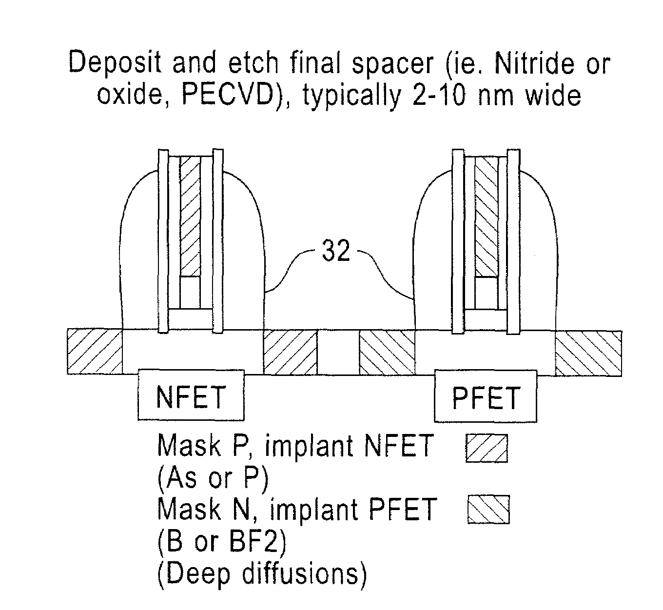
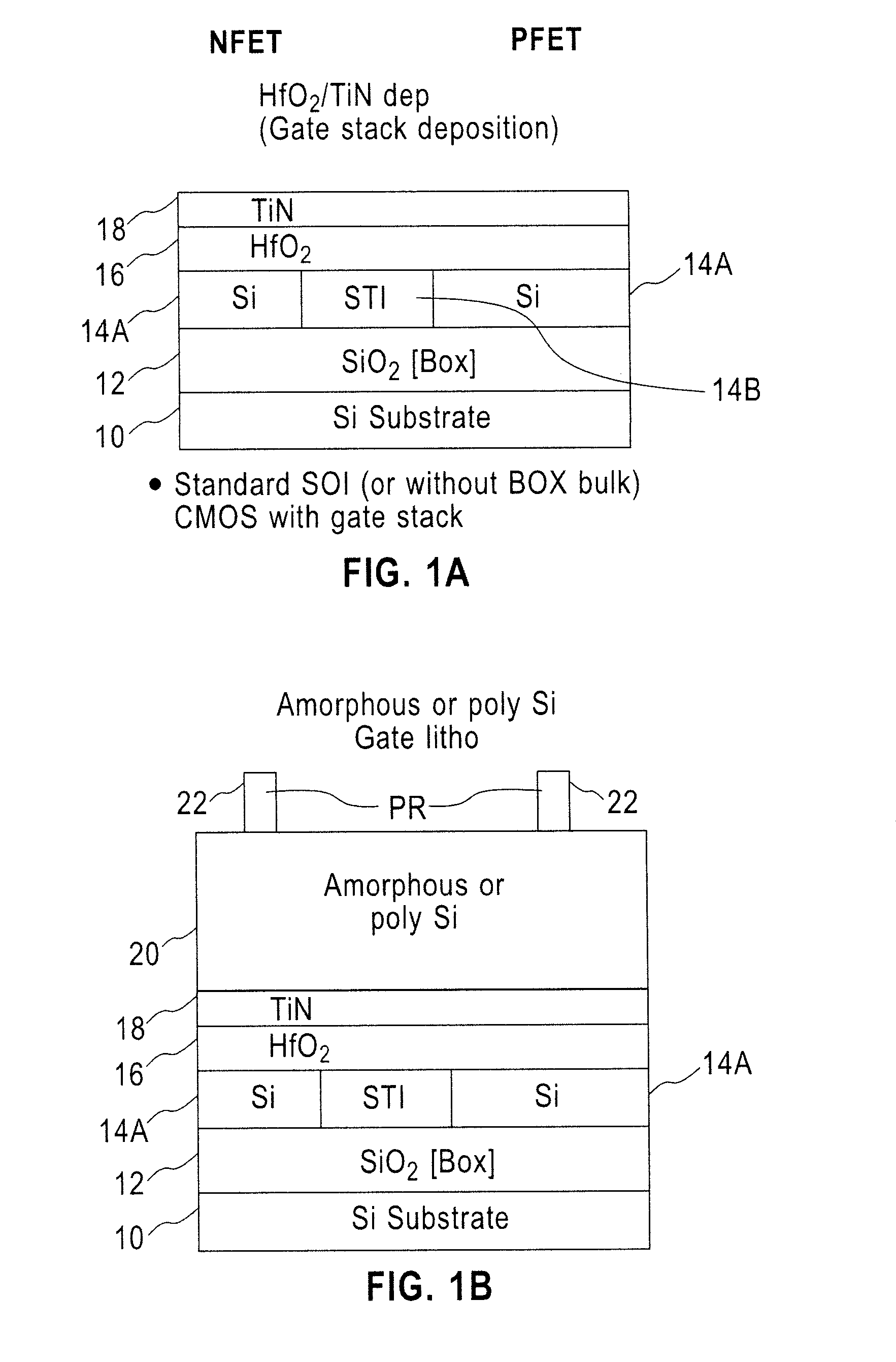
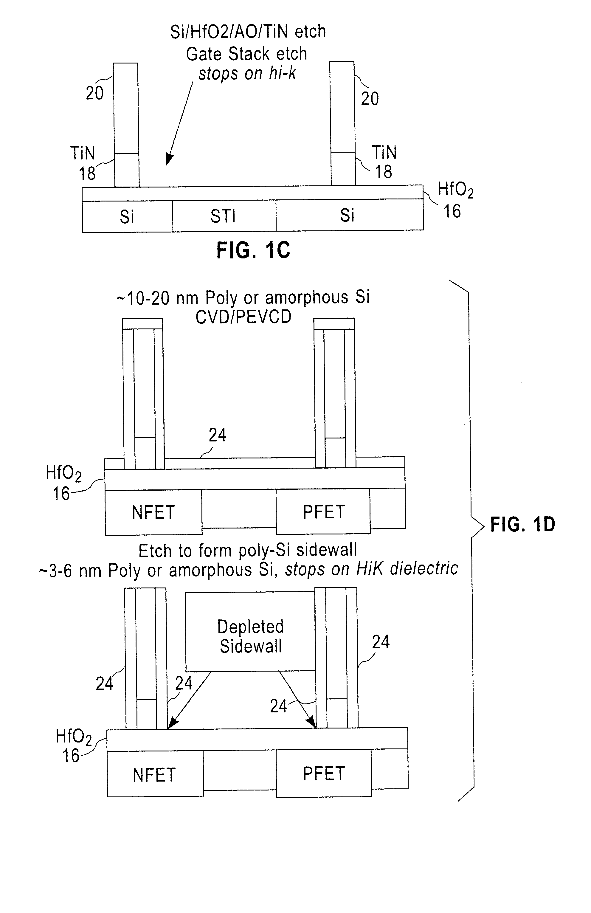
[0012]Although well-known to those skilled in the art, certain abbreviations that appear in the ensuing description and / or in the Figures are defined as follows:

BOX buried oxide

CMOS complementary metal-oxide semiconductor

CVD chemical vapor deposition

FET field effect transistor

HfO2 hafnium oxide

MLD multi-layer deposition

PECVD plasma enhanced chemical vapor deposition

PR photoresist

RIE reactive ion etch

RTA rapid thermal anneal

SOI silicon on insulator

STI shallow trench isolation

TiN titanium nitride

poly polycrystalline silicon

Si silicon

[0013]The inventors have realized that, as compared to conventional poly-gated FETs, the origin of the increased C of is due to a lack of sidewall depletion in the metal gate. This added capacitance adds to the Miller capacitance (Cmiller) and thus has a tangible performance impact. It can be determined that there can exist an approximately a 3.2% per 10 aF / μm of C of increase (assuming that N-type FETS (NFETs) and P-type FETs (PFETs) track together in Cof...


PUM

PropertyMeasurementUnit
thicknessaaaaaaaaaa
thicknessaaaaaaaaaa
thicknessaaaaaaaaaa

Abstract

A method is disclosed to reduce parasitic capacitance in a metal high dielectric constant (MHK) transistor. The method includes forming a MHK gate stack upon a substrate, the MHK gate stack having a bottom layer of high dielectric constant material, a middle layer of metal, and a top layer of one of amorphous silicon or polycrystalline silicon. The method further forms a depleted sidewall layer on sidewalls of the MHK gate stack so as to overlie the middle layer and the top layer, and not the bottom layer. The depleted sidewall layer is one of amorphous silicon or polycrystalline silicon. The method further forms an offset spacer layer over the depleted sidewall layer and over exposed surfaces of the bottom layer.

Description

TECHNICAL FIELD[0001]The exemplary embodiments of this invention relate generally to semiconductor devices and methods to fabricate them and, more specifically, exemplary embodiments of this invention relate to a class of devices known as metal high dielectric constant (high-k or MHK) transistors.BACKGROUND[0002]MHK transistors are experiencing extremely active development in the industry. One observed problem relates to the presence of an elevated outer fringe capacitance (C of), on the order of 40-80 aF / μm. The elevated value of C of is of concern, in that it at least impairs high frequency operation of the MHK transistor.[0003]In U.S. Pat. No. 7,164,189 B2 Chien-Chao Huang et al. describe a method that includes providing a semiconductor substrate including a polysilicon or a metal gate structure including at least one overlying hardmask layer; forming spacers selected from the group consisting of oxide / nitride and oxide / nitride / oxide layers adjacent the polysilicon or metal gate ...

Claims


Application Information

Patent Timeline
Patent Type & Authority Applications(United States)
IPC IPC(8): H01L21/28
CPCH01L21/823864H01L21/84H01L27/1203H01L29/6656H01L29/4966H01L29/517H01L29/66545H01L29/4908
Inventor CHANG, LELANDLAUER, ISAACMO, RENEE T.SLEIGHT, JEFFREY W.
Owner TAIWAN SEMICON MFG CO LTD
Features
  • R&D
  • Intellectual Property
  • Life Sciences
  • Materials
  • Tech Scout
  • Unparalleled Data Quality
  • Higher Quality Content
  • 60% Fewer Hallucinations
Learn More