Tunable cavity resonator and method for fabricating same

a resonator and cavity technology, applied in the direction of optical elements, optical radiation measurement, instruments, etc., can solve the problems of limited application of such resonator technology to short wavelengths (less than 1.6 m), unsuitable application types of resonator devices, and general limitations of such resonator devices, so as to achieve efficient optical generation and detection, easy modification, uniform layer uniformity and flatness

Inactive Publication Date: 2009-12-10
UNIV OF WESTERN AUSTRALIA
View PDF9 Cites 15 Cited by
  • Summary
  • Abstract
  • Description
  • Claims
  • Application Information

AI Technical Summary

Benefits of technology

[0007]MEMS represent the integration of mechanical elements, sensors, actuators, photonics and electronics on single substrates. The use of microfabrication technology employed in silicon very large scale integration (VLSI) integrated circuit technology to generate miniature three-dimensional structures such as motors, gears, accelerometers and pressure sensors on the same substrate as the associated drive and sensing electronics, has dramatically expanded the field of mechatronics. In addition to allowing mechanical manufacture on a micro-miniature scale, MEMS technology brings the low-cost, high throughput advantages of VLSI technology to mechanical and sensor systems.
[0182]Thinning and all patterning of the transferred membrane is possible thereafter by using a post transfer RIE step to etch the silicon nitride membrane 77. Such “after transferring” patterning process steps have the advantage that they allow small fragile features to be present in the final membrane which could otherwise be damaged during the flotation process.

Problems solved by technology

Further, the use of such resonator devices has generally been limited to applications in which the wavelength of resonance need only be tuned a small amount (in the order of 0.01 to 0.10 μm).
This in turn has limited the application of such resonator technology to short wavelengths (less than 1.6 μm), i.e. in wavelength regions of near IR and below.
In the context of IR filtering technology, these wavelengths are less than 2 μm, and thus these types of resonator devices are quite unsuitable for applications in the short wavelength infrared (SWIR), the mid-wavelength infrared (MWIR), the long wavelength infrared (LWIR) and visible wavelength regions.
However, the resultant membranes tend to be formed with considerable tensile stress.
Hence, it has previously been understood in the art that the use of MEMS structures in the fabrication of tunable cavity resonators is only applicable to very small wavelength applications, limiting the scope of the technology to near IR radiation and below for tunable lasers and detectors for short wavelength (e.g. less than 1500 nm optical communications) applications, and is not really suitable for longer wavelength radiation applications in the IR wavelength regions.
A concomitant problem with using high temperature deposition processes is the controllability of the intrinsic stress in the membrane during the fabrication process, quite aside from the issue of the high tensile stress that may be provided in the membrane after fabrication is completed.
Too much intrinsic tensile stress results in stiff membranes, which in extreme situations can cause membranes to fracture, whilst compressive stresses result in buckled and / or collapsed membranes.
Therefore, in any application of MEMS structure technology to longer wavelength filtering, stress control is a major problem that has to be overcome.
In these multi-layered applications, any unaccounted for residual stress can easily result in stress mismatch between the layers, leading to bowing or buckling of the released membrane.
Due to the differences in material properties and process technology, different process approaches must be used for each of these materials, significantly adding to the problem of MEMS development for systems integrating photonic devices.
However, a simple and versatile method for fabricating a tunable FP cavity device with a moveable membrane having requisite stress characteristics and quality that can be used in longer photonic wavelength applications with wavelengths extending from less than 1 micron to greater than 20 microns, and which can be fabricated at relatively low temperatures has tended to have eluded the art to date.

Method used


Image

  • Tunable cavity resonator and method for fabricating same
  • Tunable cavity resonator and method for fabricating same
  • Tunable cavity resonator and method for fabricating same

Examples


first embodiment

[0151]fabricating a tunable cavity resonator is made with reference to FIG. 7 of the drawings.

[0152]As shown in FIG. 7A, a chrome / gold layer 51 of 2 nm chrome and 50 nm gold is thermally evaporated on to a silicon substrate 53 to act as the lower reflector as well as the lower electrode of the cavity. This layer 51 is also required to promote adhesion between the zinc sulphide sacrificial layer and the silicon substrate during the PECVD process. Without this layer, the adhesion of the sacrificial layer to the silicon substrate would be so low that during the PECVD process at 300° C., thermal stresses between the two materials would cause the sacrificial layer to peel off from the substrate.

[0153]As shown in FIG. 7B, the zinc sulphide sacrificial layer 55 is then thermally evaporated onto the substrate composite of FIG. 7A, the thickness of this layer corresponding to the final relaxed cavity length of the resultant cavity resonator. During the sacrificial layer deposition, the silic...

second embodiment

[0169]Now describing the second embodiment in more detail, reference is made to FIGS. 8 and 9 of the drawings.

[0170]As shown in FIG. 8A, a Cr / Au mask layer 71 is deposited on a GaAs substrate 73. A 3 μm thick sacrificial layer of ZnS 75 is then thermally deposited onto the substrate composite of FIG. 8A, as shown in FIG. 8B.

[0171]ZnS is normally thermally deposited with high intrinsic compressive stress onto a silicon or Si substrate, as ZnS has low adhesion to Si, but adheres much better to a bare GaAs wafer with no peeling after deposition. However, during the PECVD SiNx membrane deposition process, the ZnS nonetheless sometimes peels from the substrate. This is believed to be due to the differential expansion between the two materials. Thus, the thin layer of Cr / Au 71 is first deposited on to the substrate 73 to enhance the adhesion between the ZnS and GaAs substrate, acting as a buffer layer for thermal expansion during the PECVD process and for the compressive stress present be...

third embodiment

[0185]the invention is substantially the same as the previous embodiment, without transferring the MEMS structure from the GaAs substrate to the MCT substrate, so that the final device is actually formed on the GaAs substrate.

[0186]Moreover, after the ZnS sacrificial layer is removed by wet etching, the device is rinsed and dried. The drying stage is most critical due to the adhesion effects of surface tension forces in the rinse liquid. A layer of rinse liquid is effectively trapped under the membrane (in the cavity) during the rinse process. As the device dries, this liquid evaporates causing strong surface tension forces to be exerted between the substrate and the membrane. These forces pull the membrane down into contact with the substrate when Van der Waals forces often create permanent adhesion, rendering the device useless.

[0187]To overcome this problem, the device is rinsed in distilled-deionised water followed by an acetone soak to dehydrate the device.

[0188]A rinse solutio...


PUM

PropertyMeasurementUnit
wavelengthsaaaaaaaaaa
wavelengthaaaaaaaaaa

Abstract

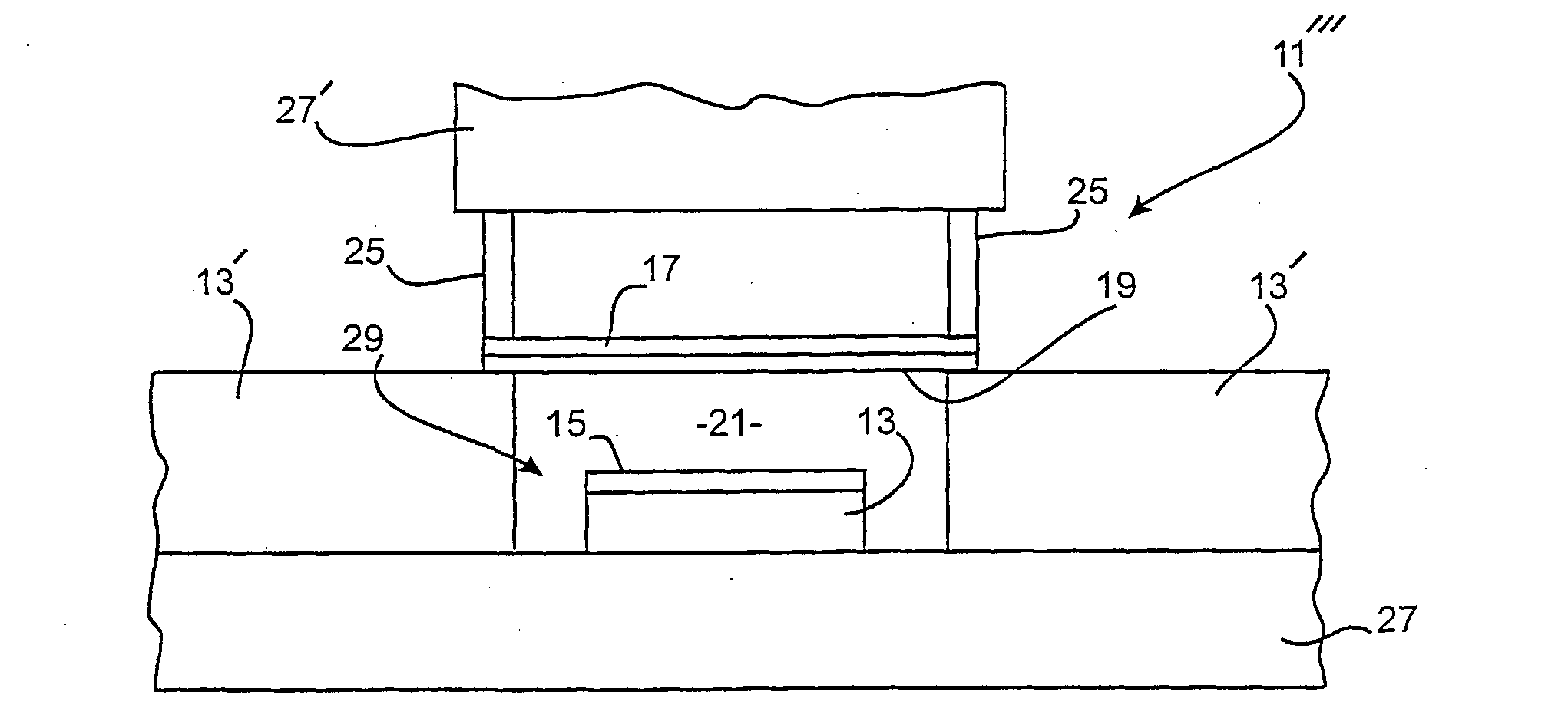
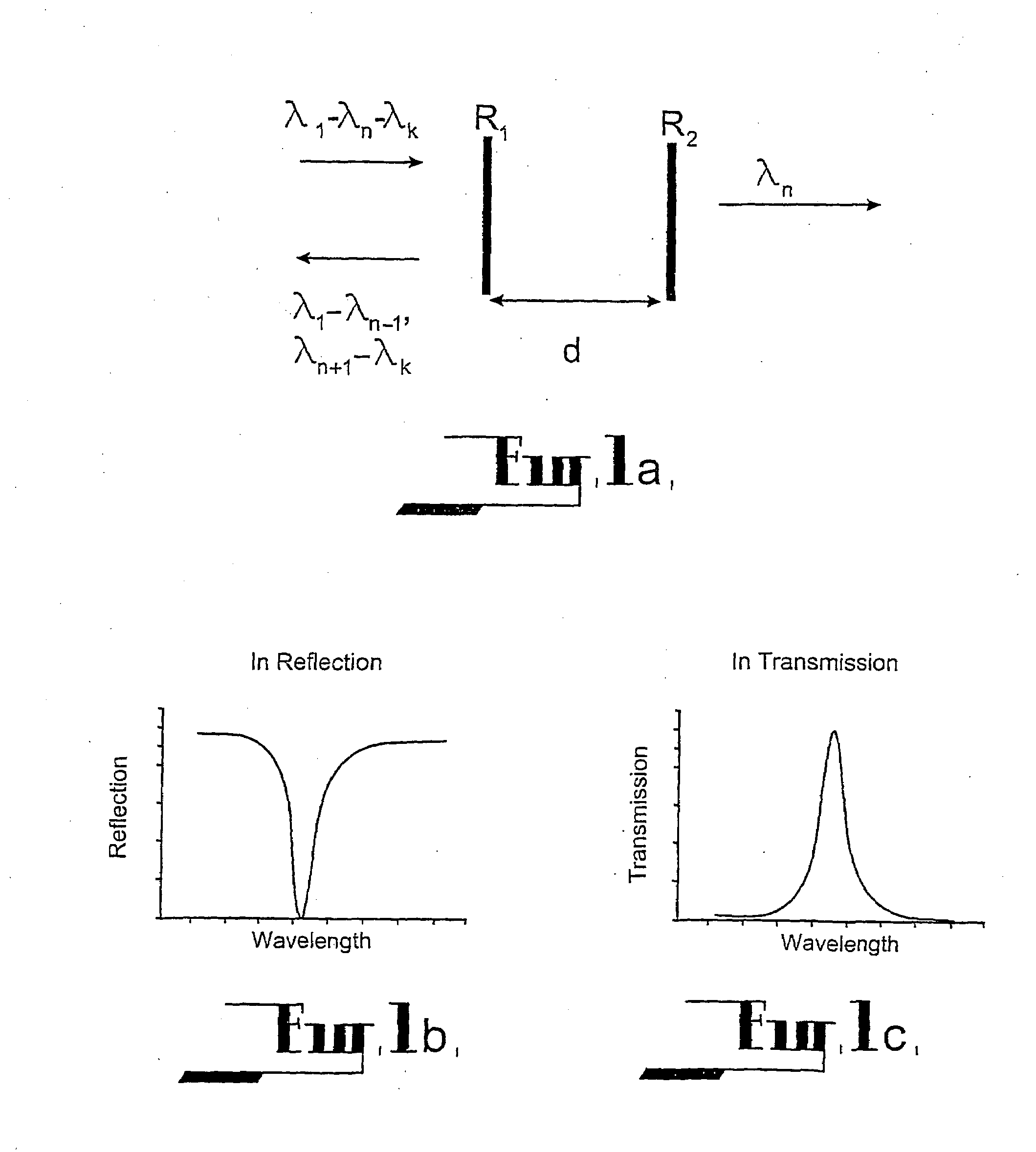
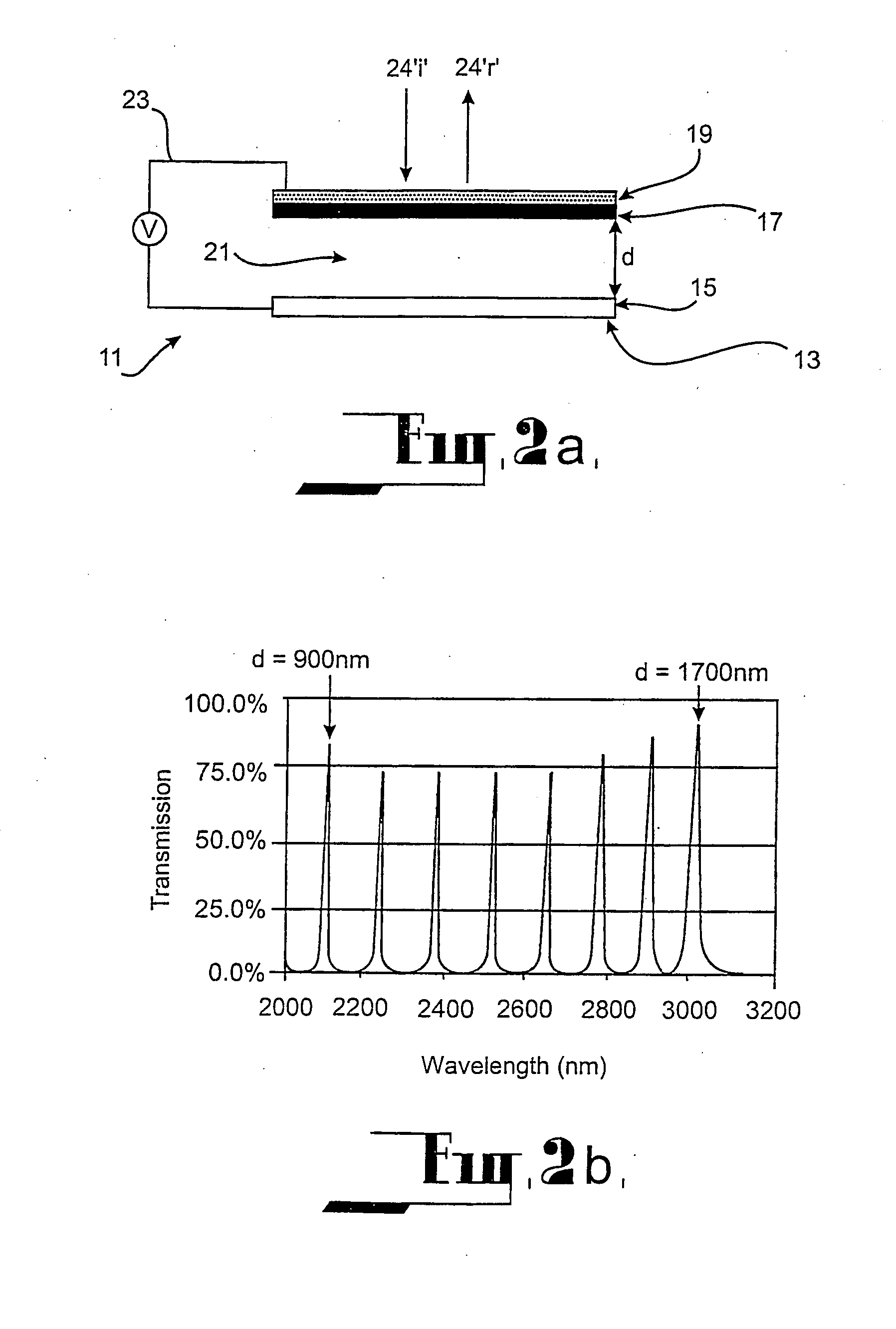
An example tunable cavity resonator for filtering radiation in the optical and IR wavelengths and an example method for fabricating same. The example resonator includes a pair of reflectors, one in fixed relationship to a substrate and the other formed upon a suspended moveable membrane disposed a cavity length from the one reflector. The resonator also includes a pair of spaced apart electrodes either constituted by the reflectors or juxtaposed therewith, which are electrostatically operable to move the membrane and other reflector relative to the one reflector.

Description

CROSS-REFERENCE TO RELATED APPLICATIONS[0001]This application is a divisional of application Ser. No. 10 / 507,015, filed Apr. 11, 2005, which is the U.S. national phase of international application no. PCT / AU03 / 00280, filed Mar. 10, 2003, which designated the U.S. and claims priority to AU application no. PS 0980 filed Mar. 8, 2002. The contents of these applications are incorporated herein in their entirety.BACKGROUND AND SUMMARY[0002]This invention relates to tunable cavity resonators utilising micro electromechanical systems (MEMS) structures in the form of deformable suspended membranes suitable for, but not limited to, photonic purposes involving infrared (IR) electromagnetic radiation, and a method for fabricating the same.[0003]The invention has particular, although not exclusive, utility in the fabrication of semiconductor devices that can be used as tunable detectors, emitters and filters for wavelength division multiplexing (WDM), micro-spectrometry and other purposes.[0004...

Claims


Application Information

Patent Timeline
Patent Type & Authority Applications(United States)
IPC IPC(8): G02B26/00C23F1/00C23C16/513H01S3/08
CPCG02B26/001G01J3/26H01S3/105H01S3/08059
Inventor FARAONE, LORENZODELL, JOHN MARCELMUSCA, CHARLES ANTHONYANTOSZEWSKI, JAREKWINCHESTER, KEVIN JAMES
Owner UNIV OF WESTERN AUSTRALIA
Why Eureka
Try Eureka