Structure to Facilitate Plating Into High Aspect Ratio Vias

a technology of high aspect ratio and structure, applied in the direction of semiconductor devices, semiconductor/solid-state device details, electrical apparatus, etc., can solve the problems of increasing the difficulty of fabricating vias, unable to meet the current the conventional fabrication process cannot keep up with the currently desirable scaled feature sizes, etc., to achieve the effect of improving the quality of high aspect ratio vias and techniques

Inactive Publication Date: 2009-12-31
TAIWAN SEMICON MFG CO LTD
View PDF18 Cites 4 Cited by
  • Summary
  • Abstract
  • Description
  • Claims
  • Application Information

AI Technical Summary

Benefits of technology

[0007]The present invention provides improved high aspect ratio vias and techniques for the formation thereof. In one aspect of the invention, a method of fabricating a copper plated high aspect ratio via is provided. The method comprises the following steps. A high aspect ratio via is etched in a dielectric layer. A diffusion barrier layer is deposited into the high aspect ratio via and over one or more surfaces of the dielectric layer. A copper layer is deposited over the diffusion barrier layer. A ruthenium layer is deposited over the copper layer. The high aspect ratio via is filled with copper plated onto the ruthenium layer.

Problems solved by technology

As the dimensions of multilayer wiring array features continue to shrink, the fabrication of vias is becoming increasingly more difficult.
Namely, conventional via fabrication processes are unable to keep up with currently desirable scaled feature sizes. FIGS. 1A-C, for example, illustrate common problems associated with conventional via fabrication processes, when smaller feature sizes (e.g., 45 nanometer (nm) node or smaller technology) are involved.
A problem with this approach is that, as the via width shrinks to below about 80 nm and the aspect (depth / width) ratio becomes larger than about 5:1, the electroplating of the structure begins to fail.
This non-uniformity is a consequence of the directional nature of the sputter deposition process coupled with the fact that a layer of Cu having a sufficient thickness so as to be continuous is required on the via bottom / sidewalls to ensure that there are no spots that cannot be plated.
As a result, when electroplating is attempted this overhang occludes the via opening and causes the via opening to close off leaving an unfilled void within in the via, which is a catastrophic fault.
Use of a Ru seed layer, however, has significant drawbacks that arise from the relatively high resistivity of Ru compared to Cu and the chemical inertness of Ru.
If only five nm of Ru are deposited, the resistivity of the resulting structure renders electroplating extremely difficult, as voltage drops across the wafer cause unacceptable non-uniformity in the Cu deposition.
One could increase the conductivity of the substrate by depositing a thicker layer of Ru, and alleviate this problem, but then the subsequent CMP process would not be possible.
One is left with a choice of problems, if the Ru is thick enough to make plating easy, subsequent CMP is not possible with the standard Cu polishing slurry.
If the Ru layer is thinned to the point where CMP becomes possible, the substrate is too resistive for uniform plating using standard techniques.
Furthermore, even if a method is developed to polish thicker layers of Ru, it would not be a desirable solution.

Method used


Image

  • Structure to Facilitate Plating Into High Aspect Ratio Vias
  • Structure to Facilitate Plating Into High Aspect Ratio Vias
  • Structure to Facilitate Plating Into High Aspect Ratio Vias

Examples


Embodiment Construction

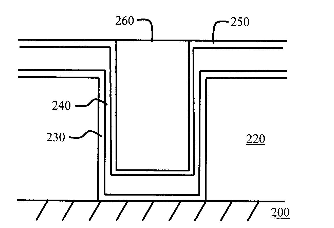
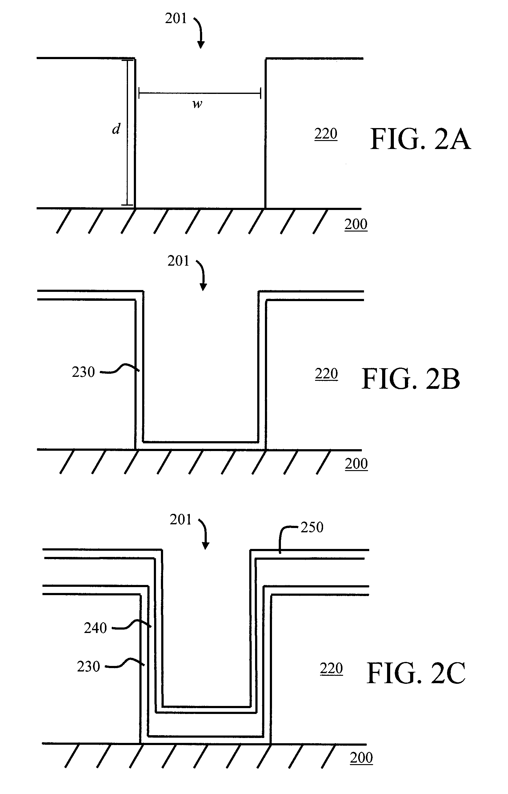
[0012]FIGS. 2A-D are cross-sectional diagrams illustrating an exemplary via fabrication process. As shown in FIG. 2A, dielectric layer 220 is deposited over substrate 200. Dielectric layer 220 can comprise any suitable dielectric material, including, but not limited to, one or more of silicon dioxide (SiO2), silicon-carbon-oxygen-hydrogen materials (e.g., SICOH) and organic polymers, and can be deposited using any suitable deposition process, such as chemical vapor deposition (CVD), atomic layer deposition (ALD), evaporation, sputtering or solution based techniques, such as spin-on coating, to a thickness of from about 10 nanometers (nm) to about 1,000 nm. Substrate 200 generally represents any wiring or contact layer in a single or multilayer wiring array. High aspect ratio via 201 is then etched into dielectric layer 220, using any suitable etching process, such as reactive ion etching (RIE). According to one exemplary embodiment, high aspect ratio via 201 is etched into dielectri...


PUM

PropertyMeasurementUnit
thicknessaaaaaaaaaa
thicknessaaaaaaaaaa
thicknessaaaaaaaaaa

Abstract

Improved high aspect ratio vias and techniques for the formation thereof are provided. In one aspect, a method of fabricating a copper plated high aspect ratio via is provided. The method comprises the following steps. A high aspect ratio via is etched in a dielectric layer. A diffusion barrier layer is deposited into the high aspect ratio via and over one or more surfaces of the dielectric layer. A copper layer is deposited over the diffusion barrier layer. A ruthenium layer is deposited over the copper layer. The high aspect ratio via is filled with copper plated onto the ruthenium layer. A copper plated high aspect ratio via formed by this method is also provided.

Description

FIELD OF THE INVENTION [0001]The present invention relates to semiconductor interconnect structures and more particularly, to improved high aspect ratio vias and techniques for the formation thereof.BACKGROUND OF THE INVENTION [0002]As the dimensions of multilayer wiring array features continue to shrink, the fabrication of vias is becoming increasingly more difficult. Namely, conventional via fabrication processes are unable to keep up with currently desirable scaled feature sizes. FIGS. 1A-C, for example, illustrate common problems associated with conventional via fabrication processes, when smaller feature sizes (e.g., 45 nanometer (nm) node or smaller technology) are involved. As shown in FIG. 1A, dielectric layer 120 is deposited over substrate 100, and via 101 is etched into dielectric layer 120. As shown in FIG. 1B, via 101 / surface of dielectric 120 are lined with diffusion barrier layer 130. The diffusion barrier layer can be tantalum nitride (TaN), or any other suitable dif...

Claims


Application Information

Patent Timeline
Patent Type & Authority Applications(United States)
IPC IPC(8): H01L23/52H01L21/4763
CPCH01L21/76843H01L21/76873H01L23/53238H01L2221/1089H01L2924/0002H01L2924/00
Inventor MCFEELY, FENTON R.YANG, CHIH-CHAO
Owner TAIWAN SEMICON MFG CO LTD
Why Eureka
Try Eureka