Field effect transistor

a field-effect transistor and transistor technology, applied in the field of field-effect transistors, can solve the problems of inability to adapt to printing processes, increase production costs, and use of such conventional processing techniques, and achieve the effects of reducing the contact resistance between the source electrode and the drain electrode, reducing the resistance of the channel due to offset, and reducing the variation

Active Publication Date: 2010-01-07
JOLED INC
View PDF7 Cites 24 Cited by
  • Summary
  • Abstract
  • Description
  • Claims
  • Application Information

AI Technical Summary

Benefits of technology

[0026]According to the present invention, a channel length which is equal to or less than the processing precision can be realized and suppression of variations can be realized, which have been the problems of conventional techniques. Moreover, contact resistances with the source electrode and the drain electrode can be lowered, and an increase in channel resistance due to offsets can be eliminated.

Problems solved by technology

However, in view of desires for display apparatuses having an increased area, a problem exists in that use of such conventional processing techniques requires tremendous production equipment and increases the production cost.
However, in current technology, these materials are subjected to film formation via vacuum processes such as a vapor phase deposition method and an evaporation method, and cannot be adapted to printing processes.
Moreover, since a relatively high process temperature is required, there are constraints on the substrate material.
For example, low-melting point materials, e.g., a plastic substrate, cannot be used.

Method used


Image

  • Field effect transistor
  • Field effect transistor
  • Field effect transistor

Examples


Embodiment Construction

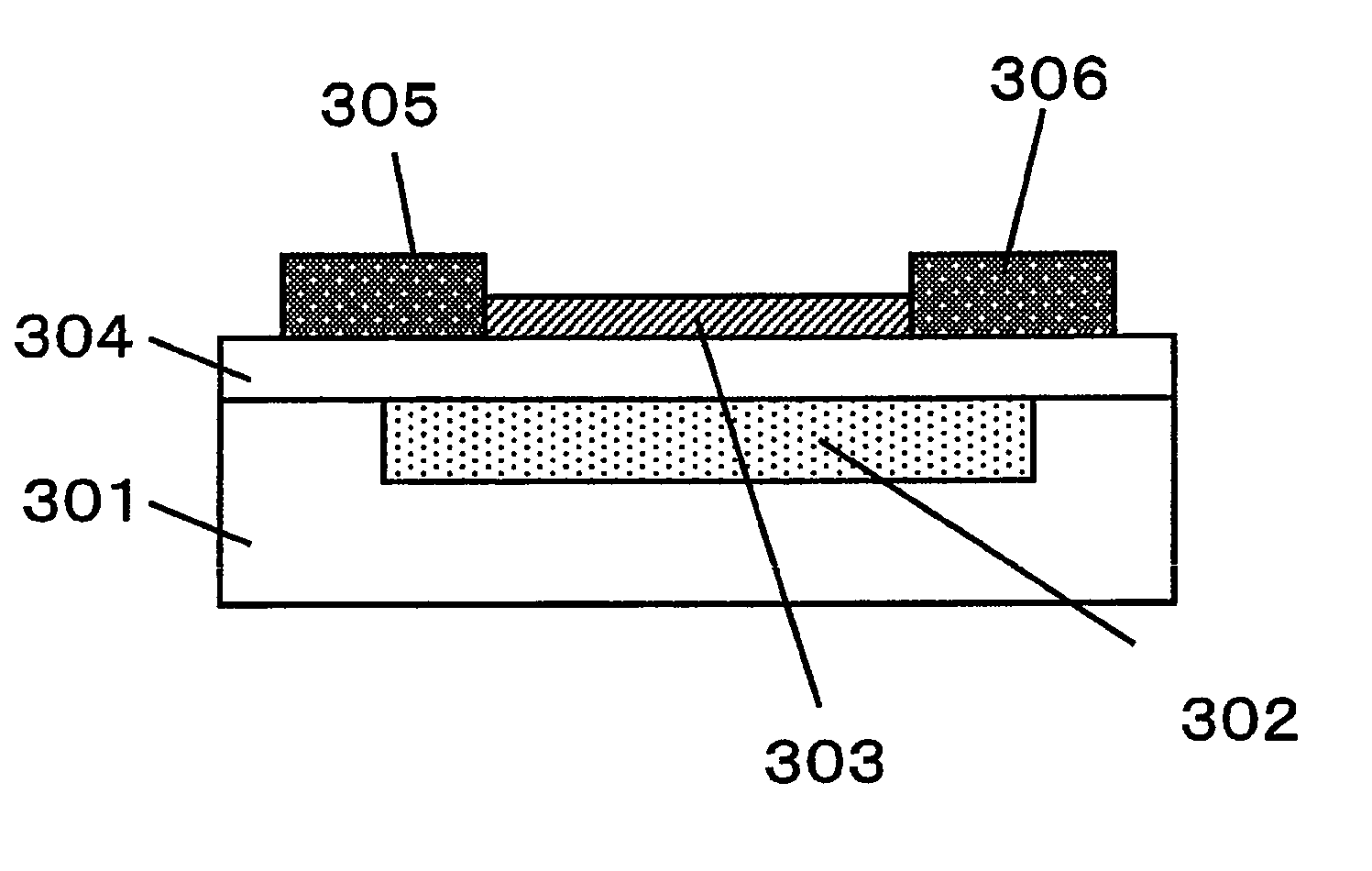
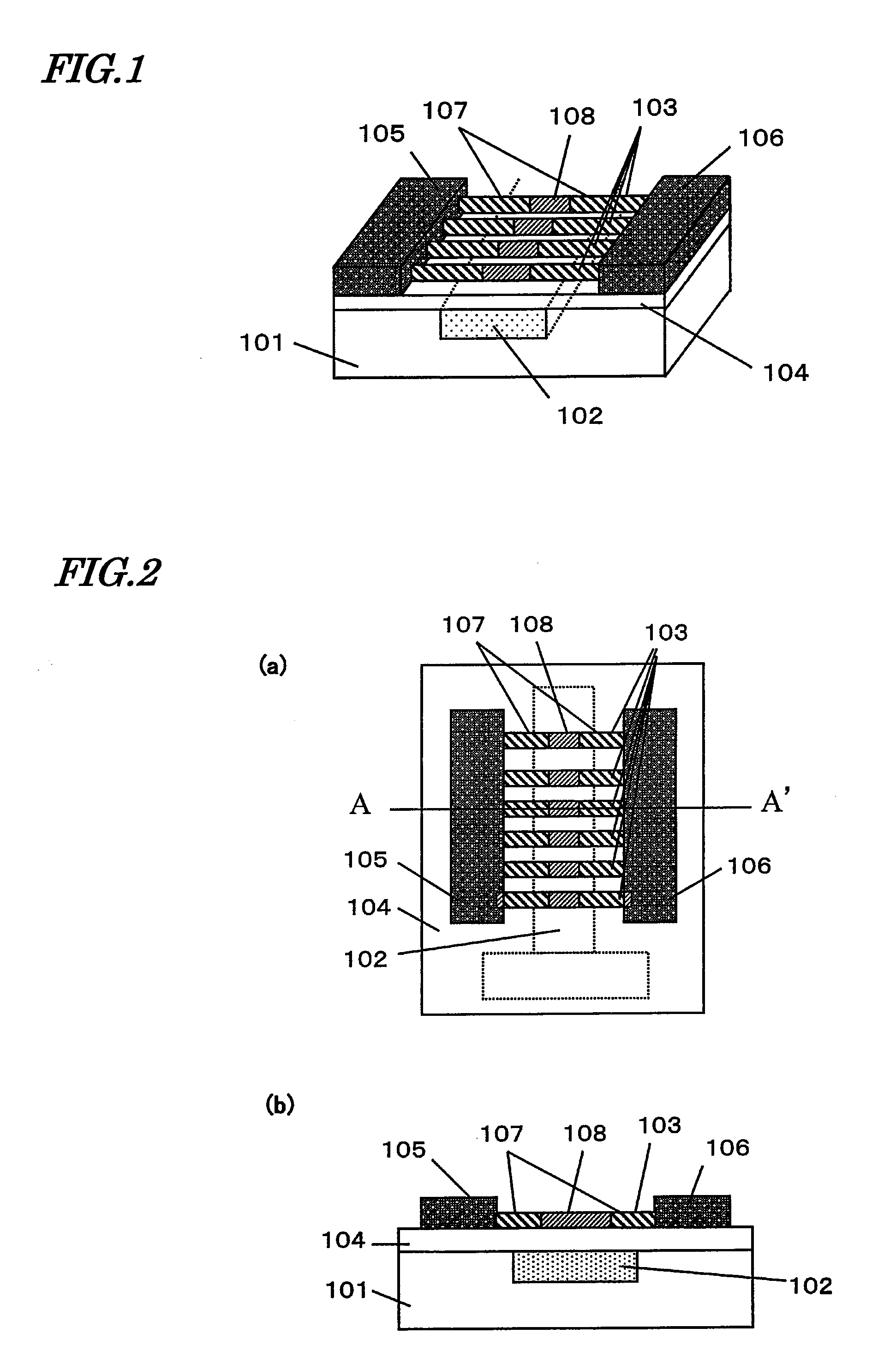
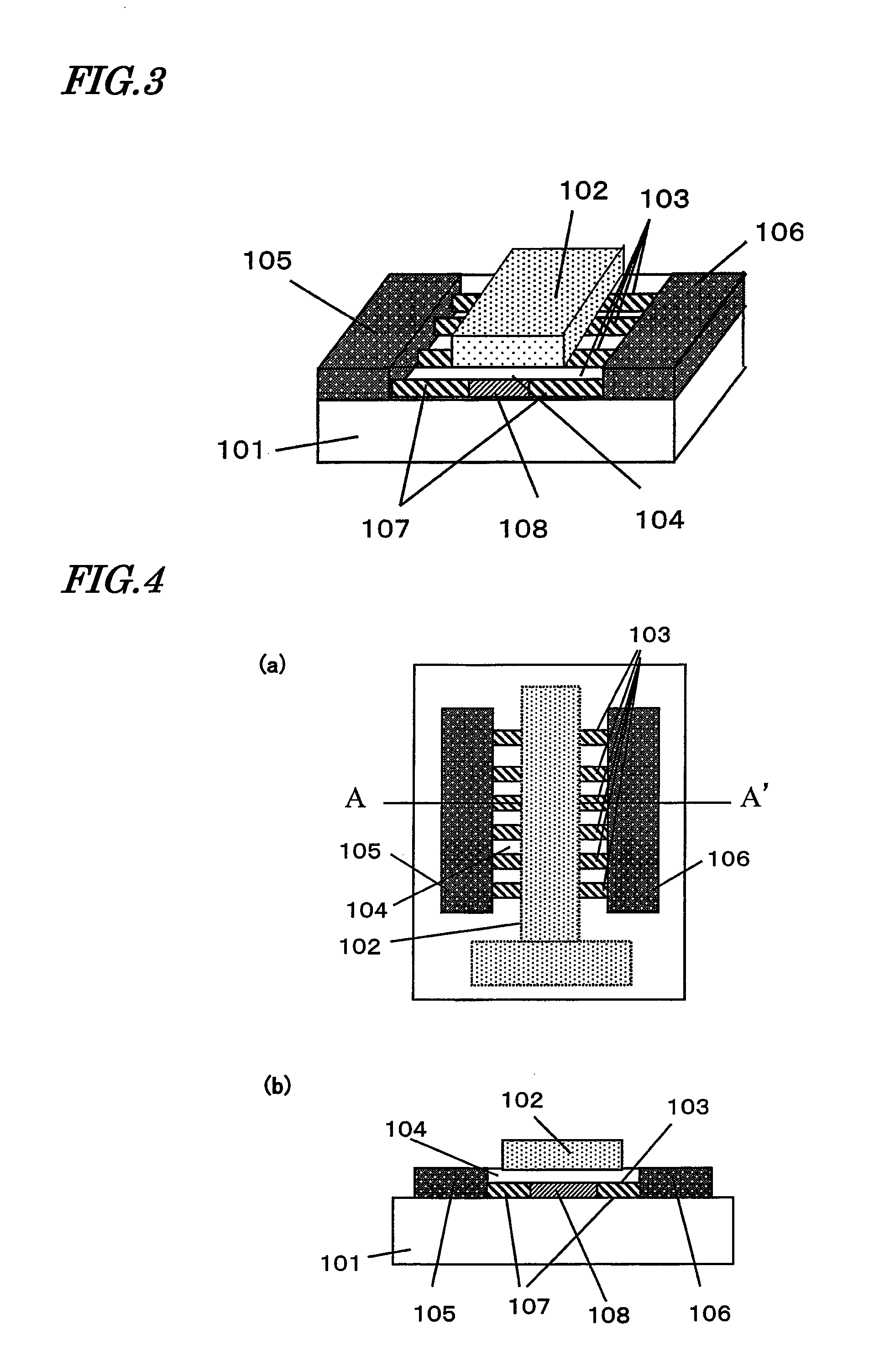
[0080]Hereinafter, with reference to the drawings, the construction of a transistor structure according to the present invention will be described. FIG. 1 shows an exemplary perspective view of a bottom-gate type transistor structure according to the present invention. FIGS. 2(a) and (b) are, respectively, an upper plan view and a cross-sectional view taken along line A-A′ of the transistor shown in FIG. 1. FIG. 3 shows an exemplary perspective view of a top-gate type transistor structure according to the present invention. FIGS. 4(a) and (b) are, respectively, an upper plan view and a cross-sectional view taken along line A-A′ of the transistor shown in FIG. 3.

[0081]It is constructed on a substrate 101, from semiconductor nanostructures 103 each having a channel layer in at least a portion thereof, a source electrode 105 and a drain electrode 106 connected to the semiconductor nanostructures 103, an insulating film 104 adjoining the semiconductor nanostructures 103 and functioning ...


PUM


Abstract

A source electrode 105 which is connected to a portion of at least one semiconductor nanostructure 103 among a plurality of semiconductor nanostructures, a drain electrode 106 connected to another portion of the semiconductor nanostructure 103, and a gate electrode 102 capable of controlling electrical conduction of the semiconductor nanostructure 103 are included. The semiconductor nanostructures 103 include a low concentration region 108 having a relatively low doping concentration and a pair of high concentration regions 107 having a higher doping concentration than that of the low concentration region 108 and being connected to both ends of the low concentration region 108. The doping concentration of the high concentration regions 107 is 1×1019 cm−3 or more; the length of the low concentration region 108 is shorter than a length of the gate electrode 102 along a direction from the source electrode 105 to the drain electrode 106; and the length of the gate electrode 102 is shorter than the interspace between the source electrode 105 and the drain electrode 106.

Description

TECHNICAL FIELD[0001]The present invention relates to a field-effect transistor, and is applicable in a broad range such as displays, logic integrated circuits, and mobile devices.BACKGROUND ART[0002]Conventionally, semiconductor processing techniques such as lithography, vacuum evaporation, and etching have been used for the fabrication of transistors which drive or control display apparatuses such as liquid crystal displays and organic electro-luminescence displays. However, in view of desires for display apparatuses having an increased area, a problem exists in that use of such conventional processing techniques requires tremendous production equipment and increases the production cost. As a means for solving such problems, transistor production methods which utilize printing technique are drawing attention, in the place of conventional semiconductor processing techniques such as lithography, vacuum evaporation, and etching. Moreover, by using a flexible substrate such as plastic...

Claims


Application Information

Patent Timeline
Patent Type & Authority Applications(United States)
IPC IPC(8): H01L29/66
CPCB82Y10/00H01L29/0665H01L29/0673H01L29/068H01L29/78696H01L29/66772H01L29/78621H01L29/78654H01L29/41733
Inventor SAITHO, TOHRUKAWASHIMA, TAKAHIRO
Owner JOLED INC
Why Eureka
Try Eureka