

Semiconductor device with amorphous silicon mas memory cell structure and manufacturing method thereof
a silicon mas and memory cell technology, applied in the field of integrated circuits, can solve the problems of difficult to reduce memory devices, difficult to reduce devices, and high cost of ic fabrication facilities, and achieve excellent scaling properties of memory devices, reduce scaling limitations, and improve signal-to-noise ratio
- Summary
- Abstract
- Description
- Claims
- Application Information
AI Technical Summary
Benefits of technology
Problems solved by technology
Method used
Image

Examples
Embodiment Construction
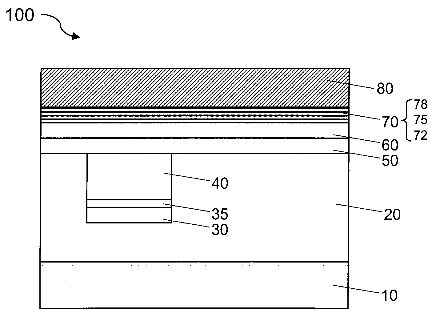
[0023]The present invention is directed to integrated circuits and their processing for the manufacture of semiconductor devices. More particularly, the invention provides a semiconductor device having a memory cell and a method for making the device. Merely by way of example, the invention has been applied to a three-dimensional (3D) amorphous silicon (a-Si) metal-aluminum oxide-semiconductor (MAS) memory cell structure and a method for the manufacture of the memory cell structure and 3D integration. But it would be recognized that the invention has a much broader range of applicability. For example, the invention can be applied to a variety of devices such as dynamic random access memory devices, static random access memory devices, Flash memory devices, and others.
[0024]As discuss above, various conventional techniques have been directed to memory cells with reduced sizes. According to one of the conventional techniques, memory cells are implemented with stacked gate structure. F...
PUM
 Abstract
Description
Claims
Application Information