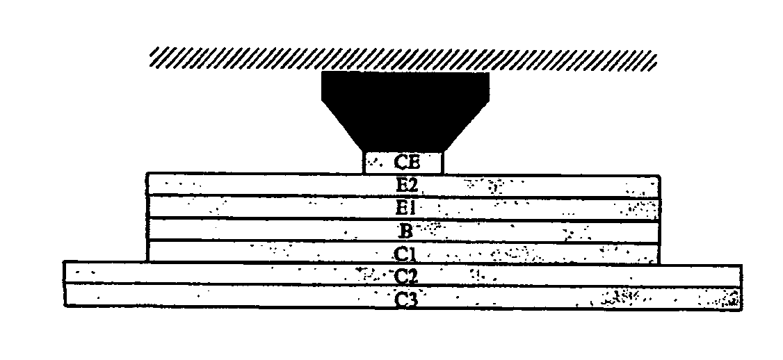
[0003]A
heterojunction bipolar transistor is made up of a stack of three
semiconductor regions: emitter, base and collector, wherein the emitter has a forbidden energy gap wider than that of the base. Its
lateral extension (in each of the planes of the preceding regions) is made up of two zones: one, called intrinsic or active, is defined by the surface of the emitter-base junction; the other, called extrinsic or parasitic, is located in the periphery of the former, between it and the
electrical contacts (base and collector) of the transistor. The speed of the HBT is optimised by jointly reducing, on the one hand, the
transit time of the carriers between the emitter and the collector and, on the other hand, the parasitic effects (serial resistors and capacitors) associated with the extrinsic zone.
Transit time can be reduced through various approaches, widely described in existing literature: ballistic injection in the base (abrupt heterojunction type I), thin base,
doping and / or
concentration gradient in the base (quasi-
electric field), thin collector, ballistic injection in the collector (type-II abrupt heterojunction), Schottky collector, etc. The reduction of parasitic effects is, in general terms, obtained by reducing the width of the
peripheral zone and by using suitable materials (i.e. low resistivity for access resistors, low electric
permittivity for the capacitors). The present invention makes it possible to reduce the base-collector capacity by means of the reduction of
transit time described above.
[0004]The invention effectively makes it possible to produce HBTs, in particular with a GaAsSb base layer, having both a thin and limited base and a deeply underetching base-collector junction. These two points, until now incompatible in the same transistor, allow for a considerable improvement of its dynamic performance. The first point mainly affects the conditions of electronic transport (band discontinuity at the emitter-base interface, effective
mass of the carriers, resistivity of the base, resistivity of the base contact, etc.) while the second point enables a drastic reduction of the base-collector parasitic capacity (i.e. associated with the extrinsic part of the base-collector junction), the parasitic capacity limiting the
operating frequency of the HBT.
[0005]GaAsSb HBTs are known from the document “Ultra-high performance staggered lineup (“Type-II”) InP / GaAsSb / InP npn Double
Heterojunction Bipolar
Transistor” C. R. Bolog nesi, M. W. Dvorak, N. Matine, O. J. Pitts and S. P. Watkins, Jpn. J. Appl. Phys. Vol. 41 Part 1(2B) 1131 (2002). These transistors have shown remarkable results (fT=fmax=300 GHz) and clear progress compared with the state of the art at the time, obtained with InP / InGaAs structures. The same authors have shown that the
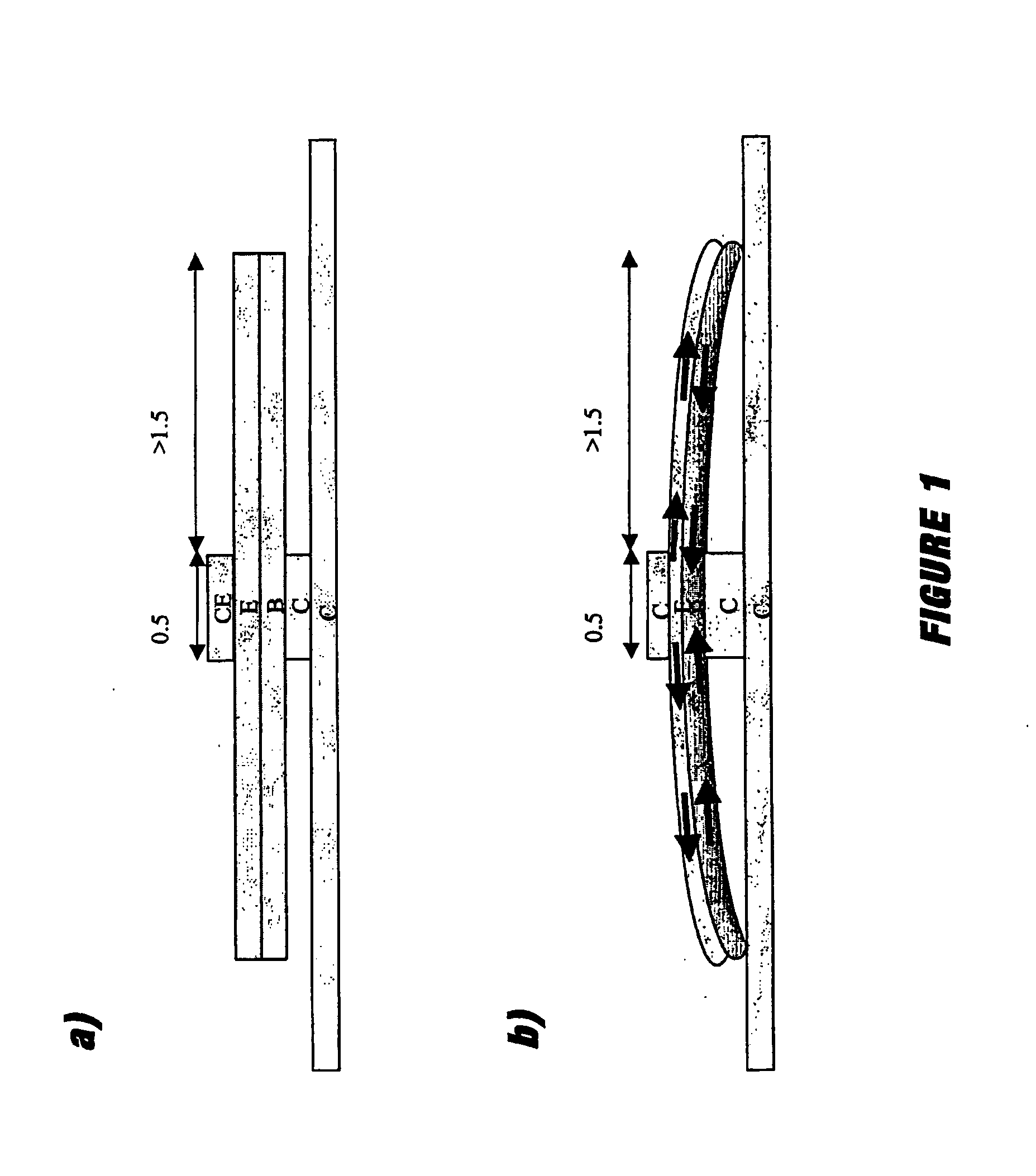
antimony composition used in the base layer was considerably lower than the concentration ensuring lattice match with InP ([Sb]=0.5). The technology used has limited the underetching of the collecting layer to 750 nm under the base contact, while the latter overhangs the emitter finger by 1.5 μm. A comparison between the experimental results and those resulting from the
simulation shows clearly superior performance (i.e. >500 GHz) for a unit report of the emitter-base and base-collector junction areas. Finally, the contribution of the GaAsSb to the speed of the transistor is clearly established.
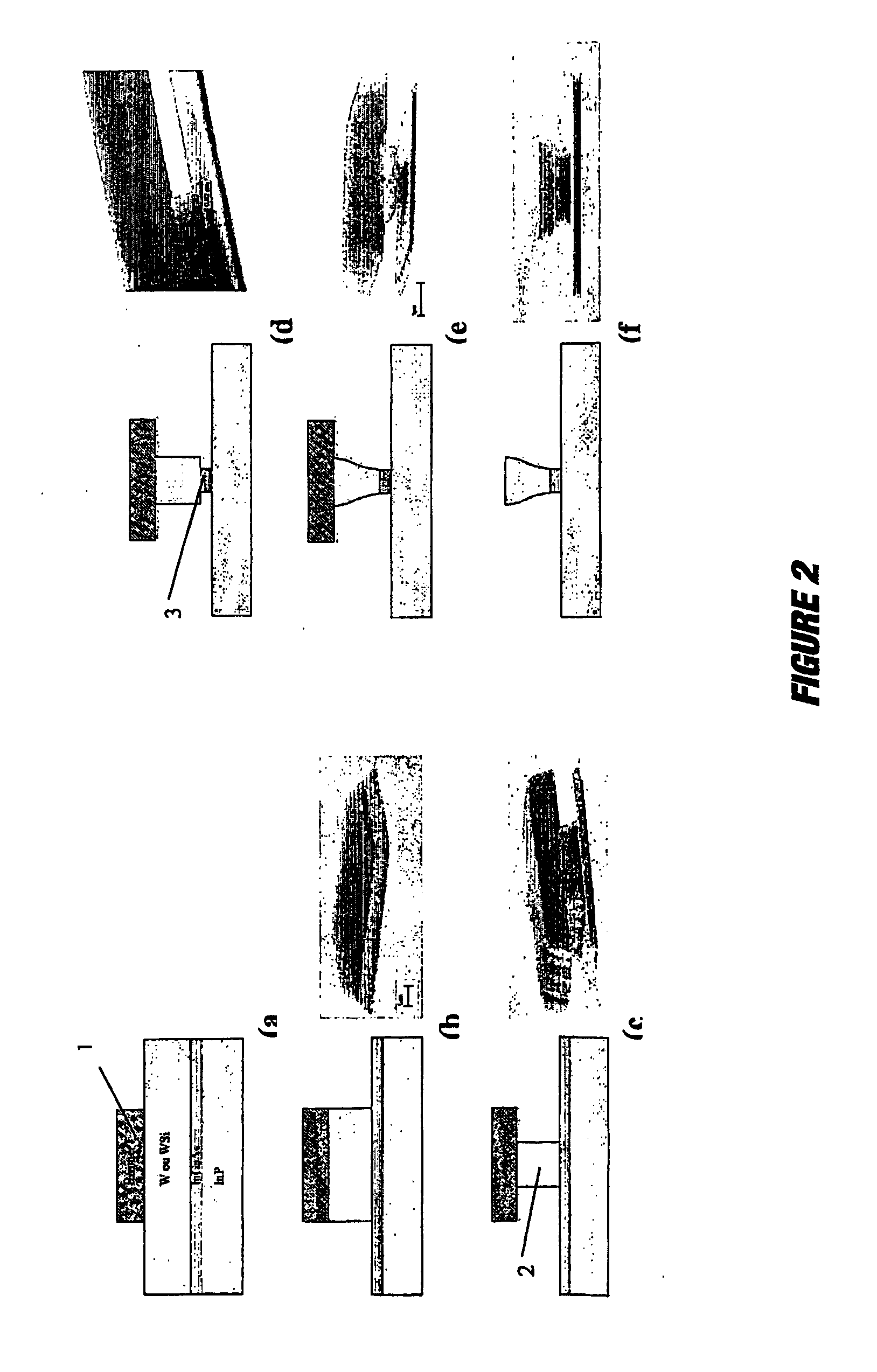
[0009]For these reasons, the skilled person in the art generally limits himself only to
etching stacks made with materials that have lattice match between them, which is to say, stacks that do not have any constraints. This is the
disadvantage that the present invention aims to solve by introducing a new layer of InGaAlAs
quaternary in the collector. The symmetry (even approximate) of the stack of
layers in the base overhang balances the constraints and considerably reduces deformations. In addition, it is known to modify the composition of the semiconductor to make the base layer, so as to considerably modify the electronic transport properties in the
active zone of the transistor.
[0010]The invention guarantees compatibility between the performance of a deep underetching and the existence of a constraint in the base layer. The invention also aims to make it possible to use, in a HBT, a base made up of a semiconductor
alloy in which the molecular arrangement (depending on the composition of the
alloy) does not correspond to the lattice match required by the emitting or collecting layer. For example, the invention supports the use of a base made from GaAsSb
alloy, with an
antimony ratio higher or lower than 50%.

