Method for manufacturing semiconductor device and semiconductor device

a manufacturing method and technology for semiconductor devices, applied in semiconductor devices, electrical devices, transistors, etc., can solve the problems of deteriorating the film quality of the gate insulating film, slowing down the progression of scaling, and the difficulty in suppressing gate leakage, so as to improve the carrier mobility, prevent crystal defects, and enhance the carrier mobility

Active Publication Date: 2010-01-07
SONY CORP
View PDF2 Cites 37 Cited by
  • Summary
  • Abstract
  • Description
  • Claims
  • Application Information

AI Technical Summary

Benefits of technology

[0036]Such a semiconductor device is manufacturing by the above-described manufacturing method. Therefore, stress is effectively applied to the above-described channel region. This feature can strain the channel region for enhancement in the carrier mobility, and can surely prevent crystal defects attributed to the existence of a high concentration of atoms having a lattice constant different from that of Si in the mixed crystal layer.
[0037]As described above, the method for manufacturing a semiconductor device and the semiconductor device according to the embodiments of the present invention allow enhancement in the carrier mobility and ensured prevention of crystal defects in a mixed crystal layer. Consequently, transistor characteristics such as the on / off ratio can be enhanced.

Problems solved by technology

However, the physical thickness of a silicon dioxide (SiO2)-based insulating film, which is used as a gate insulating film in related arts, is about to reach the limit, and therefore the technical difficulty in suppression of gate leakage is becoming particularly higher.
This causes slowdown in the progression of the scaling after the generation of the 90-nm node.
Therefore, when being subjected to high-temperature heat treatment, these metals react with a gate insulating film and so on, which causes the deterioration of the film quality of the gate insulating film.
This decreases the resistance of the surface side of the source / drain regions, and thus reduces the contact resistance.
This precludes sufficient application of compressive force to the channel region Ch, and hence suppresses enhancement in the carrier mobility.
This will result in the occurrence of problems such as the lowering of the stress and increase in junction leakage.

Method used


Image

  • Method for manufacturing semiconductor device and semiconductor device
  • Method for manufacturing semiconductor device and semiconductor device
  • Method for manufacturing semiconductor device and semiconductor device

Examples


first embodiment

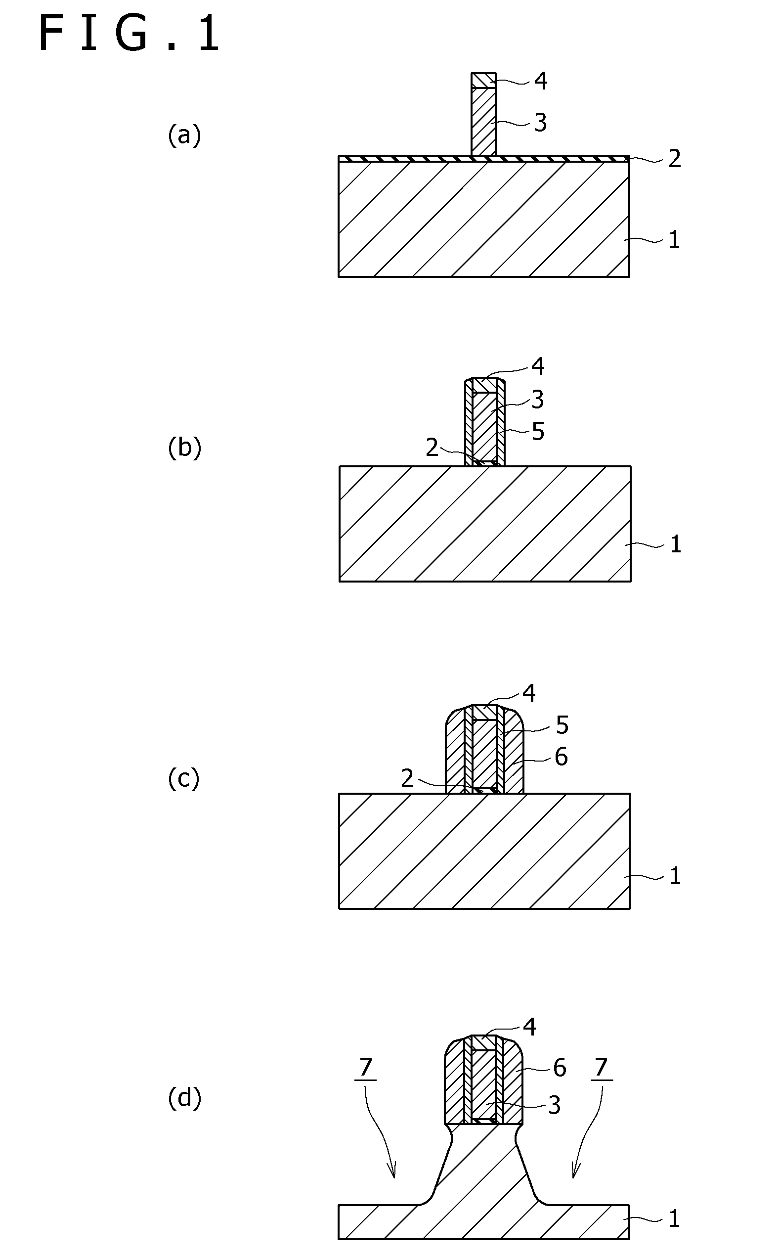
[0063]As one example of a method for manufacturing a semiconductor device according to the embodiment of the present invention, a method for manufacturing a PMOS in a CMOS (Complementary Metal Oxide Semiconductor) will be described below by using the sectional views of FIGS. 1 to 4, which show manufacturing steps.

[0064]Referring initially to (a) of FIG. 1, element isolation regions (not shown) are formed on the surface side of a silicon (Si) substrate 1 by using STI (Shallow Trench Isolation) or another method.

[0065]Subsequently, on the surface of the silicon substrate 1, a silicon dioxide (SiO2) film is deposited by e.g. oxidation as an anti-channeling protective film used for ion implantation of an impurity into the silicon substrate 1.

[0066]Thereafter, impurities are introduced by ion implantation for an NMOS transistor region and PMOS transistor region separately, for element isolation and threshold value regulation.

[0067]Subsequently, the above-described silicon dioxide film is...

working examples

[0121]Specific working examples of the embodiment of the present invention and the results of evaluation on the working examples will be described below.

working example 1

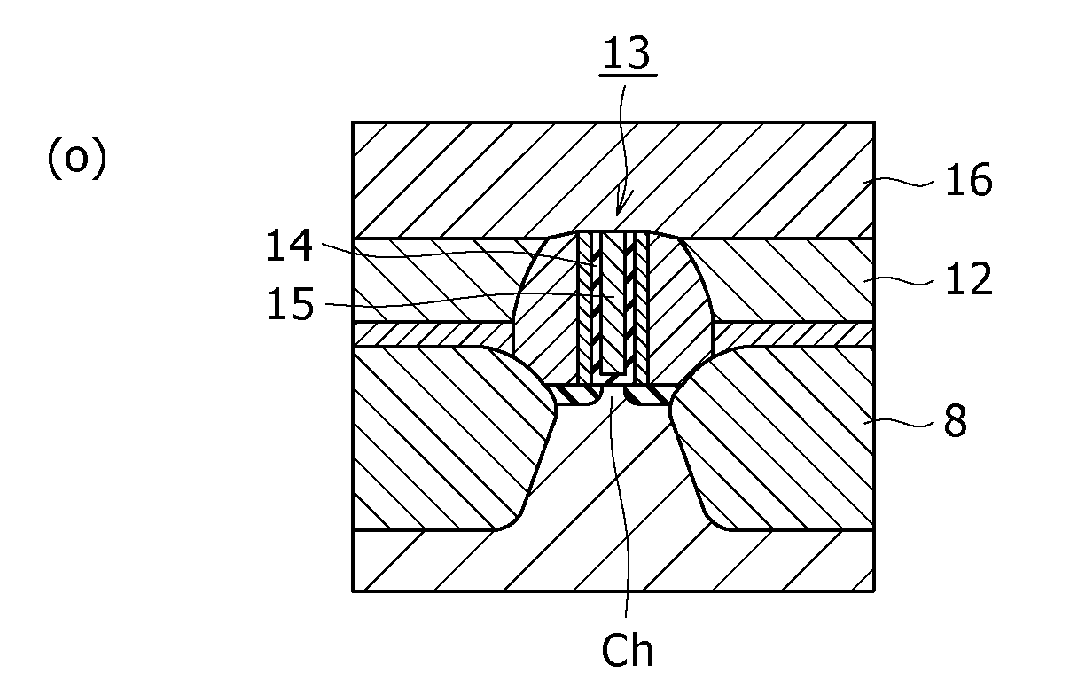
[0122]A PMOS transistor was fabricated by the same method as that of the above-described embodiment. As the gate insulating film 14, a silicon oxynitride film was used that was formed by oxidizing the surface of the silicon substrate 1 exposed at the bottom of the recess 13 by thermal oxidation and then performing nitridation treatment. For the gate electrode 15, poly-silicon (Poly-Si) was used.


PUM


Abstract

Provided is a semiconductor device manufacturing method by which sufficient stress can be applied to a channel region within allowable ranges of concentrations of Ge and C in a mixed crystal layer. A semiconductor device is also provided. A dummy gate electrode 3 is formed on a Si substrate 1. Then, a recess region 7 is formed by recess etching by using the dummy gate electrode 3 as a mask. Next, on the surface of the recess region 7, a mixed crystal layer 8 composed of a SiGe layer is epitaxially grown. Subsequently, an interlayer insulating film 12 is formed on the mixed crystal layer 8 to cover the dummy gate electrode 3, and the interlayer insulating film 12 is removed until the surface of the dummy gate electrode 3 is exposed. A recess 13 is formed on the interlayer insulating film 12 to expose the Si substrate 1 by removing the dummy gate electrode 3. Then, a gate electrode 15 is formed in the recess 13 by having a gate insulating film 14 in between.

Description

TECHNICAL FIELD[0001]The present invention relates to a method for manufacturing a semiconductor device and a semiconductor device, and particularly to a MOS (Metal Oxide Semiconductor) field effect transistor.BACKGROUND ART[0002]Along with the advancing of the generation of transistors, scaling by miniaturization is also being advanced constantly. On the roadmap of the ITRS (International Technology Roadmap for Semiconductor), it is expected that a gate length (Lg) of 20 nm or smaller will be achieved in transistors called the 32-nm node. The scaling needs to be advanced for Lg as well as for other parameters such as the equivalent oxide thickness (EOT) of a gate insulating film and the depth (Xj) of diffusion layers.[0003]The above-described scaling of the EOT is effective for ensuring of the driving capability (Ids). However, the physical thickness of a silicon dioxide (SiO2)-based insulating film, which is used as a gate insulating film in related arts, is about to reach the lim...

Claims


Application Information

Patent Timeline
Patent Type & Authority Applications(United States)
IPC IPC(8): H01L29/78H01L21/336H01L21/8238
CPCH01L21/28079H01L29/7848H01L21/823807H01L21/823814H01L21/823842H01L21/823857H01L29/165H01L29/495H01L29/4966H01L29/517H01L29/6653H01L29/66545H01L29/6659H01L29/66636H01L29/7834H01L21/28088H01L29/42312H01L29/518H01L29/45H01L29/7836H01L27/092H01L29/0847H01L29/4975H01L29/7845
Inventor TATESHITA, YASUSHI
Owner SONY CORP
Why Eureka
Try Eureka