Method for designing semiconductor integrated circuit which includes metallic wiring connected to gate electrode and satisfies antenna criterion

Inactive Publication Date: 2010-01-07
RENESAS ELECTRONICS CORP
View PDF7 Cites 8 Cited by
  • Summary
  • Abstract
  • Description
  • Claims
  • Application Information

AI Technical Summary

Benefits of technology

[0021]A method of designing a semiconductor integrated circuit, includes verifying an antenna ratio of a metallic wiring connected to a first gate electrode and the first gate electrode, based on a layout information, and computing a gate area that should be added to avoid a plasma damage to the first gate electrode, based on the verifying. The method further includes modifying a layout of the semiconductor integrated circuit, based on the computing, by arranging a logic cell having a second gate electrode having the gate area or more and is in state where the logic cell has no contribution to a logic operation of the semiconductor integrated circuit, in a free region of the layout, and connecting the second gate electrode to the metallic wiring.
[0022]In this way, since the gate area is increased by insertion of a logic cell that performs no logic operation into the free region, it is possible to improve the antenna ratio without altering other elements (logic cell arrangement and wiring) in a design object circuit.
[0024]The semiconductor integrated circuit is equipped with a first logic cell, a second logic cell, and the third logic cell. The first gate electrode in the first logic cell, the second logic cell, and the second gate in the third logic cell are connected together through the metallic wiring, and the third logic cell makes no contribution to the logic operations of the semiconductor integrated circuit. The gate area connected to the metallic wiring that functions as an antenna in the plasma process is enlarged by the second gate electrode. For this reason, the antenna ratio of the first gate electrode and the metallic wiring becomes less than or equal to an antenna criterion, which realizes a semiconductor integrated circuit in which plasma damage in the plasma process was lightened. The second gate electrode of the third logic cell that performs no logic operations is connected to a metal cell between the logic cells. Since the logic cell that performs no logic operations can be arranged in the free region, the third logic cell for improving the antenna ratio can be arranged without largely altering the layout.
[0025]According to a design method of a semiconductor integrated circuit, a manufacture method, and a manufacturing program, the plasma damage of the semiconductor integrated circuit can be lightened while controlling delay variation caused by layout correction. In addition, the plasma damage of the semiconductor integrated circuit can be controlled without increasing a circuit area.

Problems solved by technology

In such plasma processes, break down and damages of the gate insulating film caused by a charge up phenomenon (the plasma damage) have become problems.
A charge current by the electric charges captured by the signal wiring concentrates in the gate insulating film through the gate electrode and damages the gate insulating film.
However, using the standard cell which includes the protective diode will produce a problem which increases an input capacitance.
However, in a process that is minimized in the recent years, since the gate area is minute, even if the gate area is changed, the antenna ratio will hardly sufficiently change.
Since this constraint makes it difficult to predict a delaying amount of the signal wiring after alteration of the layout, there is an increased possibility that it causes a timing error in a timing verification phase.
Since arrangement and wiring length of the cells is changed, it becomes difficult to predict the delaying amount, and therefore possibility of the timing error increases.
When the timing error arises, repair processing, must be done, and consequently operation man hour and TAT (Turn Around Time) increase.

Method used


Image

  • Method for designing semiconductor integrated circuit which includes metallic wiring connected to gate electrode and satisfies antenna criterion
  • Method for designing semiconductor integrated circuit which includes metallic wiring connected to gate electrode and satisfies antenna criterion
  • Method for designing semiconductor integrated circuit which includes metallic wiring connected to gate electrode and satisfies antenna criterion

Examples


Embodiment Construction

(Outline of the Present Invention)

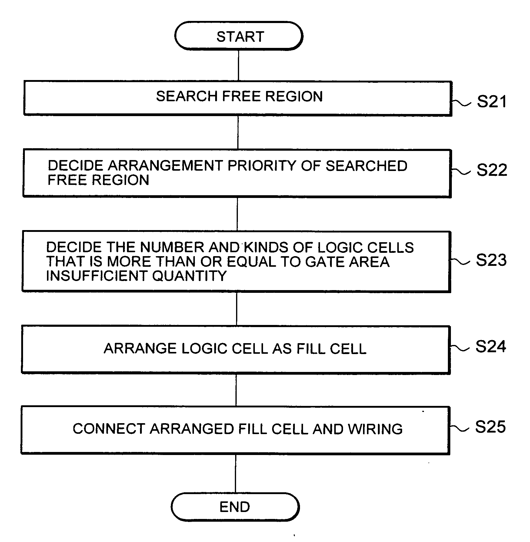
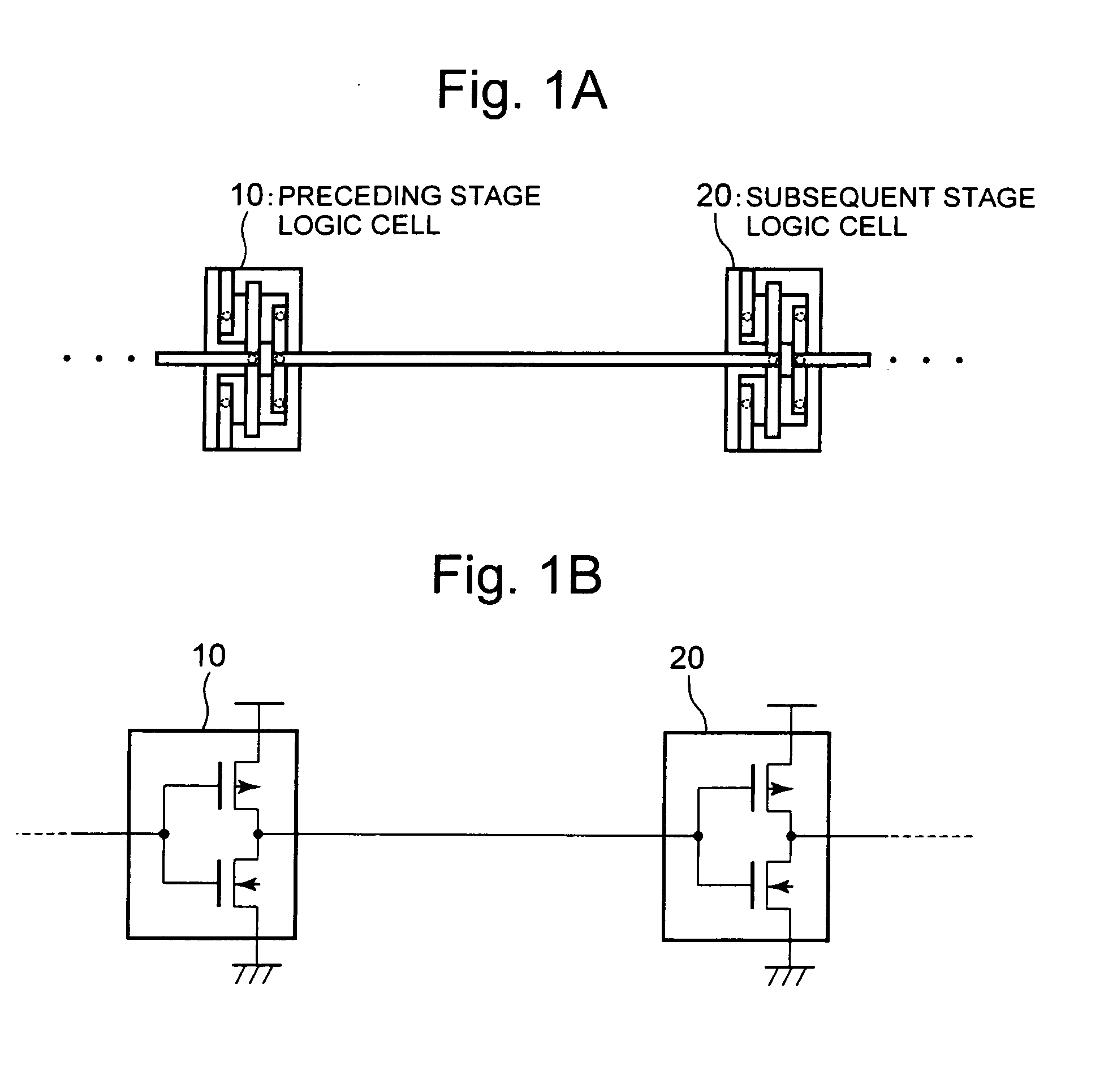
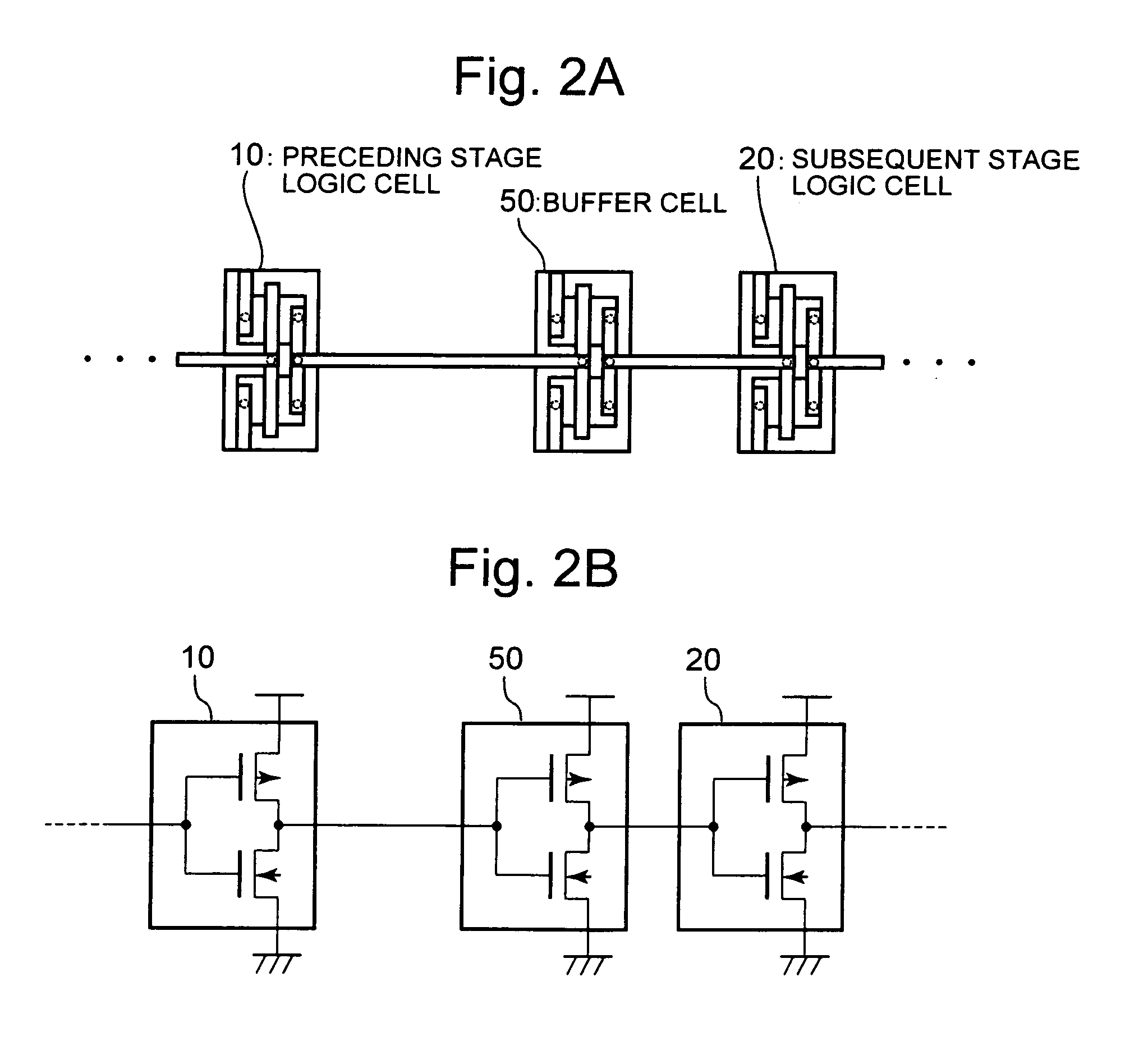
[0041]The design support system 100 verifies an antenna ratio of each transistor in a design object circuit after the chip layout in a layout phase, and corrects the layout according to the verification result. When it is determined that the antenna verification results in an antenna error in antenna ratio verification, the design support system 100 computes a gate area required in order that the antenna ratio may satisfy a predetermined criterion value (an antenna criterion), and adds a logic cell having this gate area to the design object circuit. The design support system 100 inserts the logic cell in a free region, being in a state where the logic cell to be added performs no logic operations (e.g., the output end is in an open state). A gate electrode of the transistor inside the logic cell inserted into the free region is connected to the wiring that was determined to sustain the antenna error.

[0042]In this way, since the logic cell that perfo...


PUM


Abstract

A method of designing a semiconductor integrated circuit, includes verifying an antenna ratio of a metallic wiring connected to a first gate electrode and the first gate electrode, based on a layout information, and computing a gate area that should be added to avoid a plasma damage to the first gate electrode, based on the verifying. The method further includes modifying a layout of the semiconductor integrated circuit, based on the computing, by arranging a logic cell having a second gate electrode having the gate area or more and is in a state where the logic cell makes no contribution to a logic operation of the semiconductor integrated circuit, in a free region of the layout, and connecting the second gate electrode to the metallic wiring.

Description

INCORPORATION BY REFERENCE[0001]This application is based upon and claims the benefit of priority from Japanese Patent Application No. 2008-174483 which was filed on Jul. 3, 2008, the disclosure of which is incorporated herein in its entirety by reference.BACKGROUND OF THE INVENTION[0002]1. Field of the Invention[0003]The present invention relates to a method for designing a semiconductor integrated circuit whereby plasma damage to a gate insulating film is avoided by improving an antenna ratio, a manufacture method, and a circuit design program product.[0004]2. Description of Related Art[0005]In the manufacture of thin film devices of semiconductor integrated circuits, many plasma processes, such as etching, ashing, ion implantation, and plasma CVD (Chemical Vapor Deposition), are used. In such plasma processes, break down and damages of the gate insulating film caused by a charge up phenomenon (the plasma damage) have become problems. The plasma damage occurs as follows: an electr...

Claims


Application Information

Patent Timeline
IPC IPC(8): H01L23/52G06F17/50H01L21/768H01L21/50
CPCG06F17/5072G06F2217/82H01L27/11807H01L27/0248H01L27/0207G06F30/392G06F2119/10
Inventor YODA, KENICHI
Owner RENESAS ELECTRONICS CORP
Why Eureka
Try Eureka