Semiconductor device

a technology of semiconductors and devices, applied in semiconductor devices, semiconductor/solid-state device details, electrical apparatus, etc., can solve the problems of deterioration in reliability, insufficient channel temperature, and harmful influence on long-term reliability of fet, so as to reduce the thickness of the first heat sink section, increase the thermal resistance, and increase the heat spread effect

Inactive Publication Date: 2010-01-14
NEC CORP
View PDF10 Cites 21 Cited by
  • Summary
  • Abstract
  • Description
  • Claims
  • Application Information

AI Technical Summary

Benefits of technology

[0024]In the above-described aspect of the present invention, the heat sink section may include metallic layers in at least a front surface and a back surface thereof.
[0025]In the above-described aspect of the present invention, a bonding layer may be included in an interface between the metallic layer and the heat sink section.
[0027]In the above-described aspect of the present invention, at least two directional components of the thermal conductivity of the heat sink section in X, Y and Z directions may be equal to or higher than 600 W / mK, the heat sink section having anisotropic thermal conductivity.
[0029]According to further aspect of the present invention, there is provided a semiconductor device, comprising: a semiconductor element having a rectangular two-dimensional geometry and serving as a heat source; a first heat sink section having the semiconductor element mounted thereon; and a second heat sink section joined to the opposite side of the first heat sink section having the semiconductor element, wherein a relation among directional components of thermal conductivity is: K1yy≧K1xx>K1zz, where directional components of the three-dimensional thermal conductivity of the heat sink section in X, Y and Z directions are determined as Kxx, Kyy and Kzz, and wherein a relation among directional components of thermal conductivity of the second heat sink section is K2zz≧K2yy>K2xx or K2yy≧K2zz>K2xx, where the directional components of thermal conductivity of the second heat sink section in X, Y and X directions are determined as K2xx, K2yy and K2zz.
[0032]In the above-described aspect of the present invention, a plurality of the semiconductor elements may be included, and the semiconductor elements may be aligned in series along the longer side direction of the semiconductor element.
[0034]This allows obtaining larger heat spread effect in the first heat sink section. Further, the reduced thickness of the first heat sink section allows an inhibition for the increase in the thermal resistance. Further, in the second heat sink section, the heat spread by the first heat sink section is released with an improved efficiency due to larger thermal conductivity along Z direction. In the above-described combination, such combined advantageous effect of the heat spread effect by the first layer and the higher thermal conductivity to Z direction by the second layer achieves reduced thermal resistance of the entire semiconductor device.

Problems solved by technology

When the output power density is considerably increased, a channel temperature of a field effect transistor (FET) that constitutes the amplifier is considerably increased, causing harmful influence in the long term reliability of the FET.
In general, copper (Cu) is employed as a metallic material with lower cost and better thermal conductivity, and since the linear thermal expansion coefficient of Cu is different by 3 to 6 times from the thermal expansion coefficient of the semiconductor substrate of, for example, silicon, gallium arsenide or the like, a thermal stress is exerted over the semiconductor substrate in the assembly operation, causing a problem of a deterioration in the reliability.
Since an increase in the bonding temperature due to a self heating in a high output power laser diode a light emitting diode employing a compound semiconductor such as GaAs and the like or adversely affects the reliability of the device, the chip is also mounted on the heat sink in the similar way for releasing the heat.
However, in recent years, the requirements for miniaturization and higher power are increased in the high-power amplifiers such as power amplifiers for mobile phone base stations as described above, and thus the use of heat sink materials such as CuW, CuMo and the like cannot provide sufficient channel temperature (warranty temperature: for example, about 120 to 150 degree C. for GaAs or Si) for ensuring sufficiently higher reliability in the FET.
In addition, increased power is expected in the high power laser diode or the light emitting diode, and thus a reduced thermal resistance of the heat sink is required.
This causes an increase in the difference of the thermal expansion coefficient between the heat sink and the semiconductor substrate, and an increase in the temperature during the assembly operation causes an increased thermal stress exerted over the semiconductor element, leading to a problem of deteriorating the reliability.
The use of the metallic heat sink cause a problem of a difficulty in further increasing the thermal conductivity while maintaining sufficiently smaller thermal stress in the above-described reason.

Method used


Image

  • Semiconductor device
  • Semiconductor device
  • Semiconductor device

Examples


first embodiment

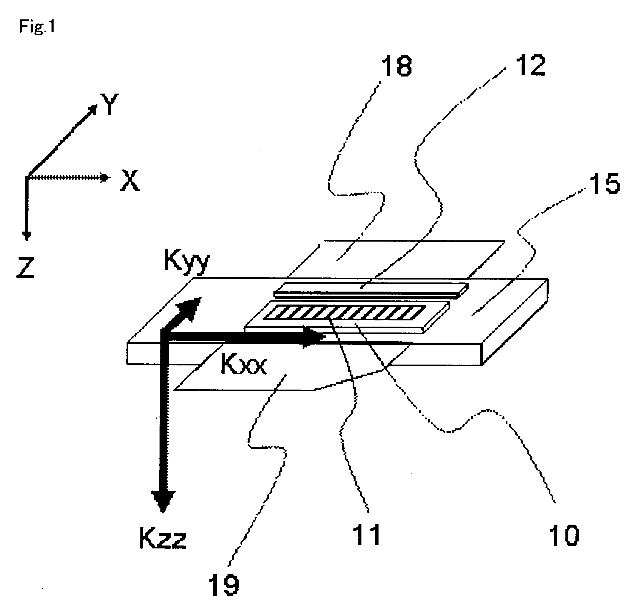
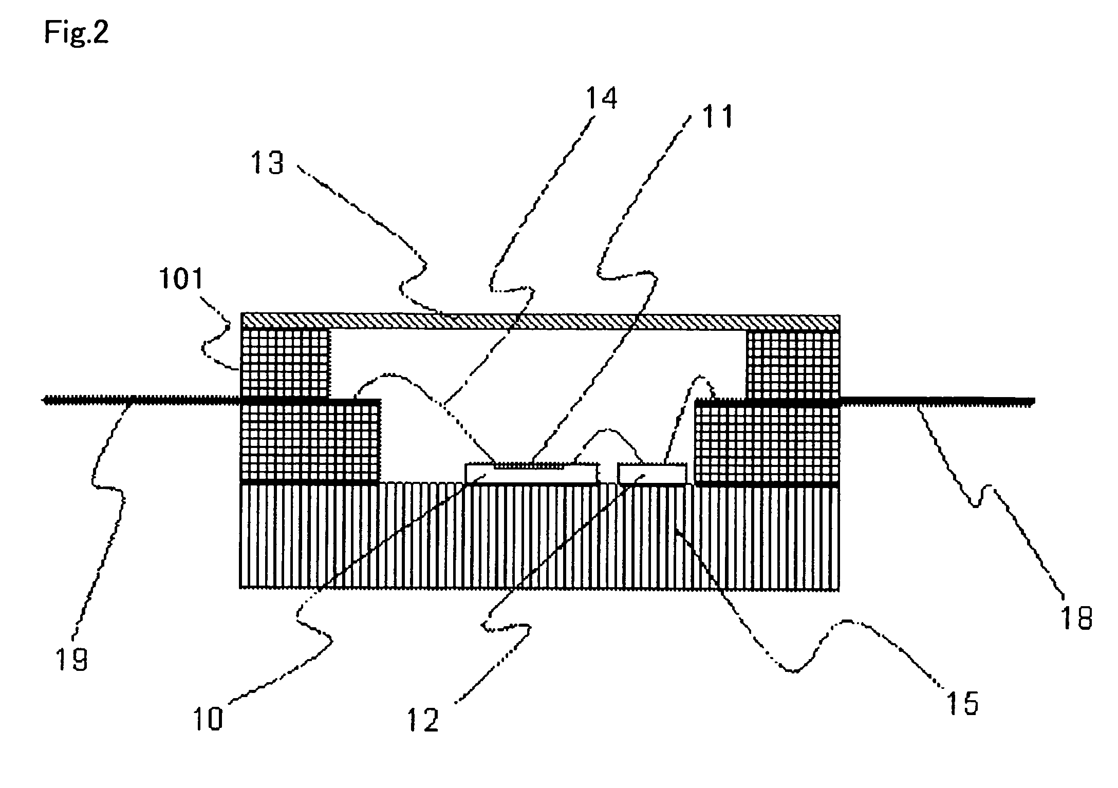
[0065]FIG. 1 is a schematic perspective view of a semiconductor device illustrating first embodiment of the present invention, and FIG. 2 and FIG. 3 are schematic cross-sectional views of semiconductor elements having rectangular two-dimensional geometry in a central section of the semiconductor element, along Y direction, which is equivalent to the short side direction. The details of the respective materials are not presented in the figures, and only sections necessary for describing the feature of the present invention are extracted to be illustrated. In FIG. 1 to FIG. 3, 10 indicates a semiconductor element, 11 indicates a region for heat generated by the semiconductor element, 12 indicates a matching circuit substrate, 13 indicates a lid of a package, 14 indicates a gold wire, and 15 indicates a heat sink section. The semiconductor element 10 has a rectangular two-dimensional geometry, and serves as a heat source. Further, in FIG. 3, copper (Cu) thin layers 151 (metallic layer)...

second embodiment

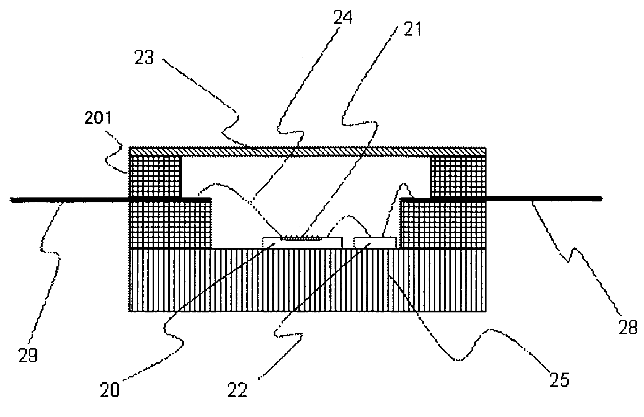
[0072]FIG. 4 is a schematic perspective view of a semiconductor device illustrating second embodiment of the present invention, and FIG. 5 and FIG. 6 are schematic cross-sectional views of semiconductor elements having rectangular two-dimensional geometry in a central section of the semiconductor element, along Y direction, which is equivalent to the short side direction. The details of the respective materials are not presented in the figures, and only sections necessary for describing the feature of the present invention are extracted to be illustrated. In FIG. 4 to FIG. 6, 20 indicates a semiconductor element, 21 indicates a region for heat generated by the semiconductor element, 22 indicates a matching circuit substrate, 23 indicates a lid of a package, 24 indicates a gold wire, and 25 indicates a heat sink section. The semiconductor element 20 has a rectangular two-dimensional geometry, and serves as a heat source. Further, in FIG. 6, copper (Cu) thin layers 251 (metallic layer...

third embodiment

[0082]FIG. 7 is a schematic perspective view of a semiconductor device illustrating third embodiment of the present invention, and

[0083]FIG. 8 and FIG. 9 are schematic cross-sectional views of semiconductor elements having rectangular two-dimensional geometry, along Y direction, which is equivalent to the short side direction.

[0084]The details of the respective materials are not presented in the figures, and only sections necessary for describing the feature of the present invention are extracted to be illustrated. In FIG. 7 to FIG. 9, 30 indicates a semiconductor element, 31 indicates a region for heat generated by the semiconductor element, 32 indicates a matching circuit substrate, 33 indicates a lid of a package, 34 indicates a gold wire, 35 indicates a first heat sink section, and 36 indicates a second heat sink section. The first heat sink section 36 is provided right under the heat source, and the second heat sink section 37 is provided around the above-described first heat s...


PUM


Abstract

A semiconductor device, comprising: a semiconductor element 20 having a rectangular two-dimensional geometry and serving as a heat source; and a heat sink section 25 having the semiconductor element 20 mounted thereon, wherein a relation among the directional components of said thermal conductivity is: Kzz≧Kyy>Kxx, where directional components of three-dimensional thermal conductivity of the heat sink section 25 in X, Y and Z directions are determined as Kxx, Kyy and Kzz, and where the longer side direction of the semiconductor element 20 is defined as X direction, the shorter side direction thereof is defined as Y direction and the thickness direction is defined as Z direction.

Description

TECHNICAL FIELD[0001]The present invention relates to a semiconductor device, and relates particularly to a high output power amplifier, a high output laser diode, light emitting diode, and the like, which are employed in a mobile phone base station, a satellite communication, radar and the like.RELATED ART[0002]High output power amplifiers employing semiconductors such as silicon (Si), gallium arsenide (GaAs), gallium nitride (GaN) and the like are widely applied in power amplifiers for mobile phone base stations or power amplifiers for mounting in a satellite and the like. Higher output power exceeding 100 W is demanded for the amplifier in these applications. On the other hand, miniaturization is required for these amplifiers, resulting in an increased output power density. When the output power density is considerably increased, a channel temperature of a field effect transistor (FET) that constitutes the amplifier is considerably increased, causing harmful influence in the long...

Claims


Application Information

Patent Timeline
Patent Type & Authority Applications(United States)
IPC IPC(8): H01L23/34
CPCH01L23/367H01L23/373H01L2924/1305H01L2924/12041H01L2924/1306H01L2924/014H01L2924/01019H01L24/48H01L2924/16195H01L2924/1423H01L2924/14H01L2924/13091H01L2924/13055H01L2924/10329H01L2924/01082H01L2924/01079H01L2924/01078H01L23/66H01L24/45H01L24/49H01L25/072H01L2223/6644H01L2224/45144H01L2224/48091H01L2224/48095H01L2224/48137H01L2224/48247H01L2224/49H01L2924/01002H01L2924/01004H01L2924/01006H01L2924/01013H01L2924/01014H01L2924/01015H01L2924/01029H01L2924/0103H01L2924/01031H01L2924/01033H01L2924/01042H01L2924/01047H01L2924/01049H01L2924/0105H01L2924/01074H01L2924/00014H01L2924/00H01L2924/351
Inventor KURODA, NAOTAKAWAKEJIMA, AKIOTANOMURA, MASAHIROMIYAMOTO, HIRONOBU
Owner NEC CORP
Why Eureka
Try Eureka