Cu alloy wiring film, TFT element for flat-panel display using the cu alloy wiring film, and cu alloy sputtering target for depositing the cu alloy wiring film

Active Publication Date: 2010-01-21
KOBE STEEL LTD
View PDF45 Cites 16 Cited by
  • Summary
  • Abstract
  • Description
  • Claims
  • Application Information

AI Technical Summary

Benefits of technology

[0038]A Cu alloy wiring film according to the present invention makes it possible to use Cu, which has been hardly usable because of the poor adhesiveness to a glass substrate in spite of the low electrical resistivity, as a wiring material having a high adhesiveness to a glass substrate. Further, a TFT element for a flat-panel display according to the present invention that uses the above Cu alloy wiring film makes it possible: not only to use Cu of a low electrical resistivity as a wiring material; but also to improve the adhesiveness to a glass substrate composing the liquid crystal display device of a flat-panel display,

Problems solved by technology

As a liquid crystal display is getting larger in size and higher in image quality however, the electrical resistance of the wiring film increases, problems such as signal delay, electric power loss, and others appear, and therefore copper (Cu) of a lower electrical resistivity than aluminum (Al) draws attention.
Problems such as peel off do not appear even when an Al wiring film is formed directly on a glass substrate.
When a Cu wiring film is formed on a glass substrate however, the problem has been that the Cu wiring film peels off from the glass substrate since the adhesiveness between glass and Cu is poor.
However arising new problems have been that not only a process to form a high-melting-point metal layer as the primary layer is added but also, since two different metals of Cu and the high-melting-point metal are layered, corrosion occurs at the interface between Cu and the high-melting-point metal when a chemical solution is applied for etching and a desirable cross-sectional shape of the wiring film (it is considered that the desirable taper angle is 45 to 60 degrees) is not formed because of the difference of the etching rates in the layers.
Another problem has been that a process related to forming patterns of the Cu wiring film by using an etching liquid suitable for each of the layers has to be added in order to form a desirable cross-sectional shape of the wiring film and thereby the production cost of a liquid crystal panel increases.
Even by this technology however, it is very difficult to adjust the cross-sectional shape of a wiring film.
Moreover, the electrical resistivity of Cr is 12.9×10⁻⁶ Ω·cm, which is higher than the electrical resistivities of Cu and Al-2 atomic % Nd, and

Method used


Image

  • Cu alloy wiring film, TFT element for flat-panel display using the cu alloy wiring film, and cu alloy sputtering target for depositing the cu alloy wiring film
  • Cu alloy wiring film, TFT element for flat-panel display using the cu alloy wiring film, and cu alloy sputtering target for depositing the cu alloy wiring film
  • Cu alloy wiring film, TFT element for flat-panel display using the cu alloy wiring film, and cu alloy sputtering target for depositing the cu alloy wiring film

Examples


examples

[Peel off Rate Measurement Test]

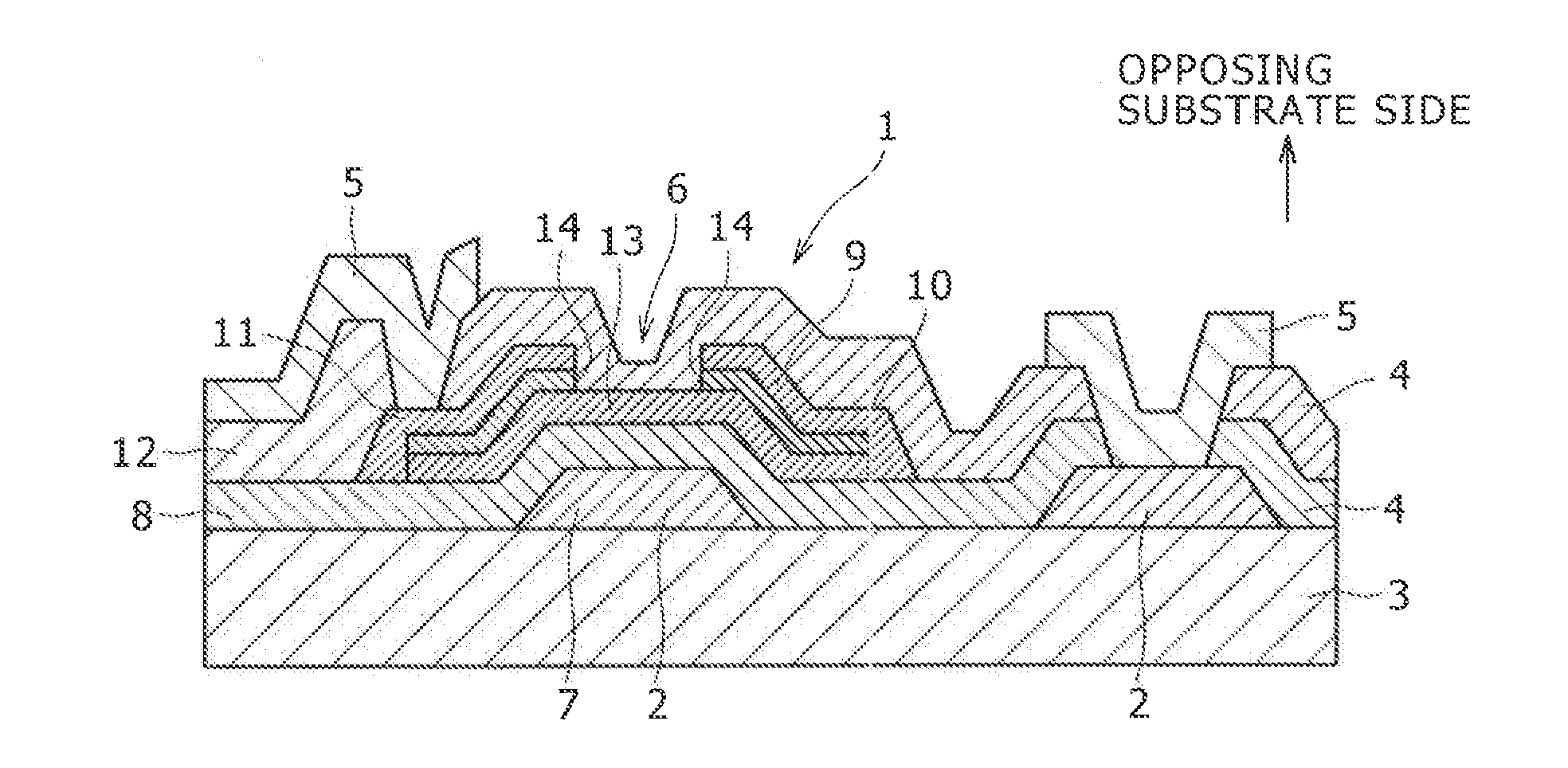
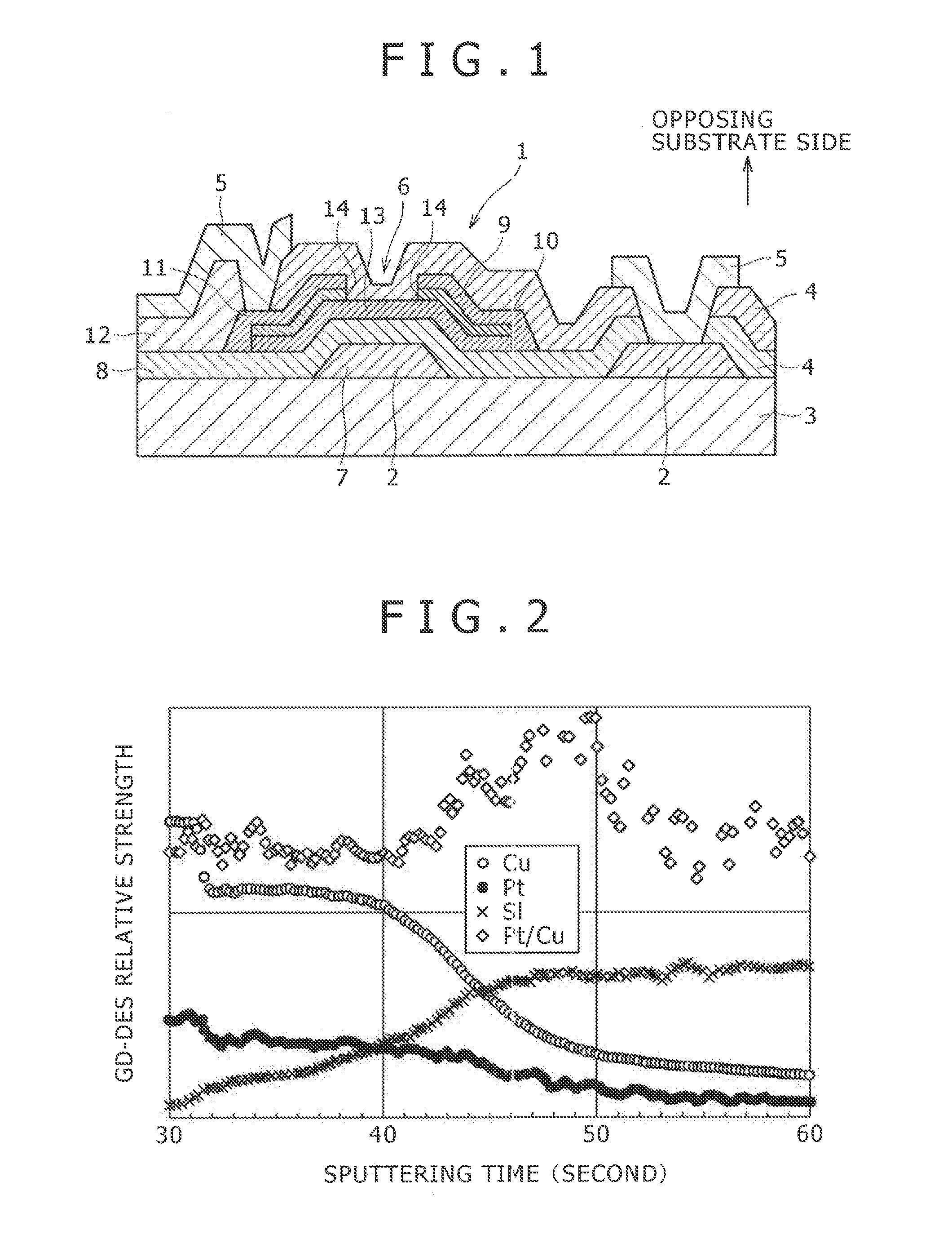
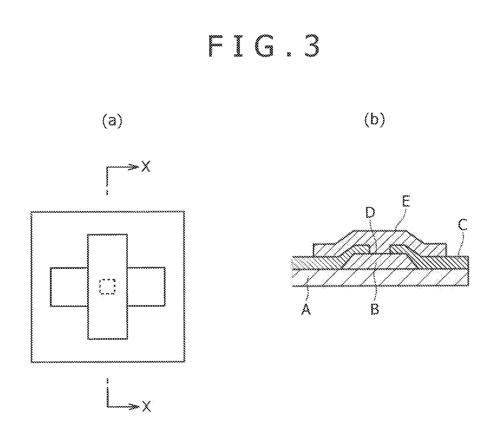
[0075]In order to evaluate the adhesiveness of a wiring film on a glass substrate, firstly the peel test of a wiring film is carried out with an adhesive tape as shown below.

[0076]In the test, a glass substrate #1737, 0.7 mm in thickness, made by Corning Incorporated is used. As the wiring film, a Cu thin film 300 nm in thickness is vapor-deposited at room temperature (25° C.) by the DC magnetron sputtering method. The Cu thin film is deposited with a sputtering target of a pure Cu on which a chip of an additional metal element is mounted. Slits are formed on the surface of a formed wiring film with a cutter knife so as to form a grid at intervals of 1 mm. Successively, an adhesive tape is put on the thin film and peeled off at a stroke while the peeling off angle of the adhesive tape is kept at 60 degrees, the number of the segments peeled off by the adhesive tape in the grid is counted, and the ratio of the number to the total number of the segment ...


PUM

PropertyMeasurementUnit
Percent by atomaaaaaaaaaa
Temperatureaaaaaaaaaa
Contact resistanceaaaaaaaaaa

Abstract

An object of the present invention is to provide: a Cu alloy wiring film that makes it possible to use Cu having a low electrical resistivity as a wiring material, exhibit a high adhesiveness to a glass substrate, and avoid the danger of peel off from the glass substrate; a TFT element for a flat-panel display produced with the Cu alloy wiring film; and a Cu alloy sputtering target used for the deposition of the Cu alloy wiring film.
The present invention is a wiring film 2 composing a TFT element 1 for a flat-panel display and a sputtering target used for the deposition of the film and the material comprises Cu as the main component and at least one element selected from the group consisting of Pt, Ir, Pd, and Sm by 0.01 to 0.5 atomic percent in total. The wiring film 2 is layered on a glass substrate 3 and further a transparent conductive film 5 is layered thereon while an insulating film 4 is interposed in between.

Description

TECHNICAL FIELD [0001]The present invention relates to: a Cu alloy wiring film composing a TFT element for a flat-panel display such as a liquid crystal display, an organic electroluminescence display, or the like; a TFT element for a flat-panel display produced by using the Cu alloy wiring film; and a Cu alloy sputtering target used for the deposition of the Cu alloy wiring film.BACKGROUND ART [0002]A liquid crystal display is explained as a representative of flat-panel displays that have come to be widely adopted in recent years. A liquid crystal display is used widely in applications ranging from a portable phone to a large-size television exceeding 100 inches. Such a liquid crystal display is categorized into a simple matrix liquid crystal display and an active matrix liquid crystal display by the method for driving pixels. In the two kinds of liquid crystal displays, the active matrix liquid crystal display incorporating a thin film transistor (abbreviated as TFT in this descri...

Claims


Application Information

Patent Timeline
IPC IPC(8): H01L29/786H01L23/48C23C14/34
CPCC22C9/00C22C9/06C23C14/3414G02F2001/136295G02F2202/28H01B1/026H01L27/124H01L23/53233H01L29/4908H01L2924/12044H01L2924/0002H01L21/32051H01L2924/00G02F1/136295
Inventor HINO, AYATOMIHISA, KATSUFUMIGOTOU, HIROSHIONISHI, TAKASHI
Owner KOBE STEEL LTD
Why Eureka
Try Eureka