Processing end point detection method, polishing method,and polishing apparatus

a technology of polishing end point and detection method, which is applied in the direction of semiconductor/solid-state device testing/measurement, lapping machines, instruments, etc., can solve the problems of large loss, circuits are not separated well, and circuit resistance can increase, so as to achieve accurate polishing end point detection, suppress the influence of noise, and average film thickness

Active Publication Date: 2010-01-21
KIOXIA CORP +1
View PDF68 Cites 46 Cited by
  • Summary
  • Abstract
  • Description
  • Claims
  • Application Information

AI Technical Summary

Benefits of technology

[0044]According to the present invention, by adjusting the rotational speed of the polishing table and the rotational speed of the top ring, the sensor does not scan only local areas, but scans substantially the entire surface of the workpiece evenly in the predetermined measuring time. As a result, an average film thickness can be grasped while an influence of noise is suppressed. Therefore, an accurate polishing end point detection and uniform film thickness can be realized.

Problems solved by technology

In this case, if the Cu layer in the interconnect trenches is excessively polished off together with the insulating film, a circuit resistance can increase and the entire substrate has to be discarded, resulting in a large loss.
On the other hand, if the Cu layer is polished insufficiently and remains on the insulating film, circuits are not separated well and short-circuit occurs.
As a result, polishing of the Cu layer should be performed again, resulting in an increased manufacturing cost.
However, in the above-described conventional methods, it is difficult to detect a distinctive point (i.e., a point of distinctive change in the reflection intensity or the characteristic value) which serves as an index indicating a polishing end point.
This makes it difficult to detect an accurate polishing end point.
Moreover, it is difficult to correct the manner of appearance.
However, selection of an optimum wavelength for a structure of a workpiece entails trial and error.
As a result, a lot of time is needed for the selection process.
Moreover, it is difficult to verify whether the wavelength selected is best suited.
However, the intensity of the reflected light from the surface of the substrate varies intricately depending not only on the change in film thickness as a result of polishing, but also on the patterns and structures of the devices.
In such a case, even if smoothing of the signal is performed, the change in film thickness cannot be accurately monitored because the noise is large.
Use of such a plating apparatus can present a problem of variations in film thickness along the periphery of the substrate because of variations in contact resistance of the cathode electrodes or because of sealing performance of the seal member.
As a result, the sensor may scan only thick portions or thin portions of the film depending on times during polishing, thus failing to measure an average film thickness.

Method used


Image

  • Processing end point detection method, polishing method,and polishing apparatus
  • Processing end point detection method, polishing method,and polishing apparatus
  • Processing end point detection method, polishing method,and polishing apparatus

Examples


Embodiment Construction

[0072]Embodiments of the present invention will be described in detail below with reference to the drawings.

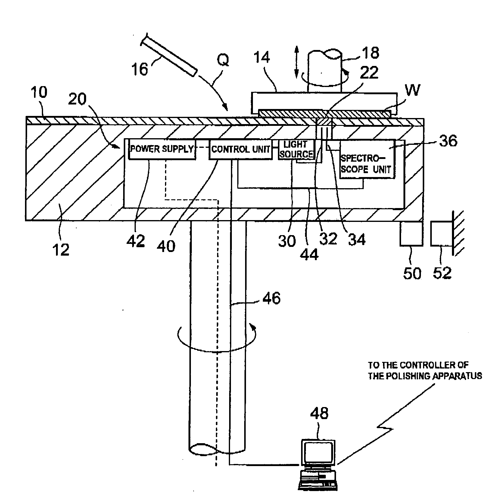
[0073]FIG. 1 is a schematic view showing an overall arrangement of a polishing apparatus capable of performing a method of detecting a polishing end point according to an embodiment of the present invention. As shown in FIG. 1, the polishing apparatus has a polishing table 12 with a polishing pad 10 attached to an upper surface thereof, and a top ring 14 for holding a substrate W, which is a workpiece (object to be polished) and pressing the substrate W against an upper surface of the polishing pad 10. The upper surface of the polishing pad 10 serves as a polishing surface providing a sliding contact with the substrate W. An upper surface of a fixed abrasive plate containing fine abrasive particles (made of CeO2 or the like) fixed by a binder, such as resin, may be used as a polishing surface.

[0074]The polishing table 12 is coupled to a motor (not shown) disposed therebelow, a...


PUM

PropertyMeasurementUnit
sizeaaaaaaaaaa
reflection intensitiesaaaaaaaaaa
wavelengthsaaaaaaaaaa

Abstract

The present invention relates to a processing end point detection method for detecting a timing of a processing end point (e.g., polishing stop, changing of polishing conditions) by calculating a characteristic value of a surface of a workpiece (an object of polishing) such as a substrate. This method includes producing a spectral waveform indicating a relationship between reflection intensities and wavelengths at a processing end point, with use of a reference workpiece or simulation calculation, based on the spectral waveform, selecting wavelengths of a local maximum value and a local minimum value of the reflection intensities, calculating the characteristic value with respect to a surface, to be processed, from reflection intensities at the selected wavelengths, setting a distinctive point of time variation of the characteristic value at a processing end point of the workpiece as the processing end point, and detecting the processing end point of the workpiece by detecting the distinctive point during processing of the workpiece.

Description

TECHNICAL FIELD[0001]The present invention relates to a processing end point detection method for detecting a timing of a processing end point (e.g., polishing stop, changing of polishing conditions, etching stop, film-formation stop, and the like) by calculating a characteristic value of a surface of a workpiece (an object of polishing) such as a substrate.[0002]The present invention also relates to a polishing method and polishing apparatus for polishing a substrate, such as a semiconductor wafer, to planarize the substrate.BACKGROUND ART[0003]The trend of recent years in a semiconductor device has been a highly integrated structure, which requires fine interconnects and multi-layered structure. To realize the fine interconnects and the multi-layered structure, it is necessary to planarize a surface of a substrate. Chemical mechanical polishing (CMP) is conventionally used to remove irregularities from the surface of the substrate to thereby planarize the surface.[0004]In the chem...

Claims


Application Information

Patent Timeline
Patent Type & Authority Applications(United States)
IPC IPC(8): B24B49/04B24B49/12B24B37/04B24B37/013B24B37/10B24B49/10H01L21/304
CPCB24B37/013B24B49/12B24D7/12G01N21/55G01N21/9501H01L22/26B24B49/16H01L2924/0002G01B11/0675G05B19/406G05B19/4065B24B49/04H01L2924/00H01L21/304H01L22/00
Inventor SHIMIZU, NOBURUOHTA, SHINROMARUYAMA, KOJIKOBAYASHI, YOICHIMITANI, RYUICHIRONAKAI, SHUNSUKESHIGETA, ATSUSHI
Owner KIOXIA CORP
Why Eureka
Try Eureka