
Semiconductor photo detector

a technology of photo detector and semiconductor, applied in the direction of semiconductor devices, basic electric elements, electrical appliances, etc., can solve the problems of difficult understanding of design and manufacture conditions, acquiring manufacture tolerance, etc., and achieve the effects of reducing the level of generated dark current, reducing the electric field, and reducing the interface of passivating film 112

Inactive Publication Date: 2010-01-28
NEC CORP
View PDF2 Cites 13 Cited by
  • Summary
  • Abstract
  • Description
  • Claims
  • Application Information

AI Technical Summary

Benefits of technology

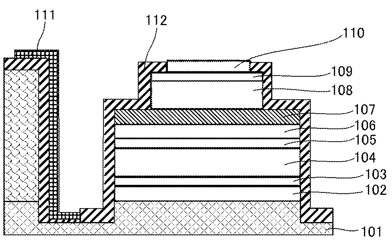
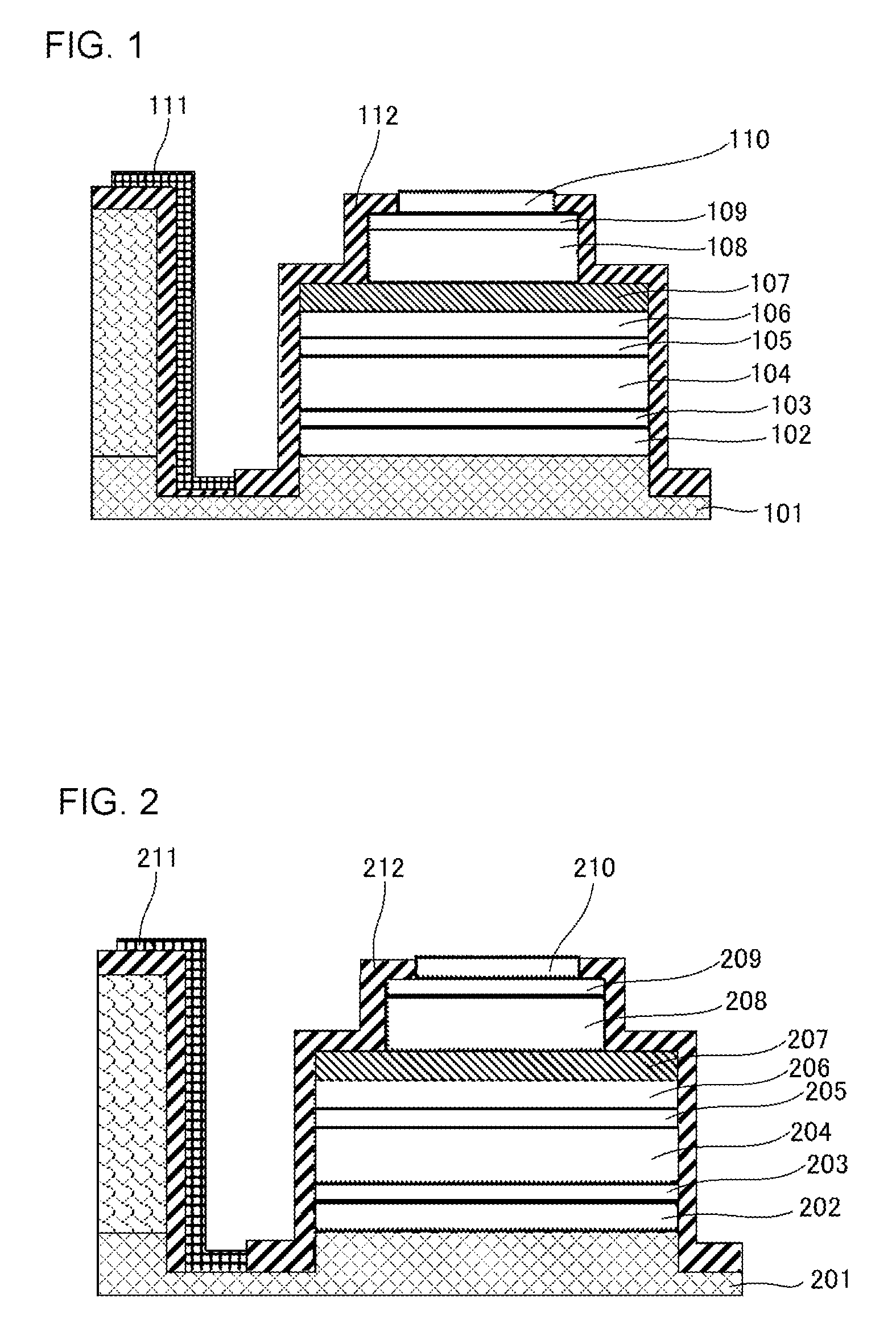
[0048]As shown in FIG. 1, according to the invention of the present exemplary embodiment, light may be entered through the first mesa including the electrode 110 in the side of the second-type conductivity, the contact layer 109 of the second-type conductivity and the buffer layer 108 of the second-type conductivity in the semiconductor photo detector of the mesa structure, and the light may be received by the light absorption layer 106 of the second-type conductivity contained in the second mesa located outside of the circumference of the first mesa in two-dimensional view. Alternatively, light may be entered through the substrate 101 and received by the light absorption layer 106. In such case, a light reflected by the electrode 110 of the second-type conductivity may also be received with the light absorption layer 106. When an appropriate voltage is applied to the element for the operating voltage, the electric field of the side wall section having the passivating film 112 can be reduced over the light absorption layer 106 of the second-type conductivity and the underlying undoped layer (multiplication layer 104) and the regions of the layers of the first-type conductivity (selective etching layer 102 of the first-type conductivity and field-relaxing layer 103 of the first-type conductivity), and thus the electric field over the side wall of the second mesa and the side wall of the first mesa is relatively reduced, as compared with the section right under the first mesa, causing a difficulty in the flow of electric current. Therefore, electric current flowing through the interface in the passivating film 112 is relatively reduced, and thus a deterioration of the interface in the passivating film 112 is reduced, ensuring the long term reliability of the semiconductor photo detector.
[0049]While the electric field distribution in the depleted layer is a single-dimensional distribution in the conventional mesa-structure semiconductor photo detector illustrated in FIG. 6, an equipotential surface of the depleted layer is modulated in the photosensitive semiconductor element of first exemplary embodiment. More specifically, the electric field right under the outer circumference (or side wall) of the buffer layer of the second-type conductivity is increased over the regions of the light absorption layer of the second-type conductivity and the first field-relaxing layer, and the multiplier layer, as compared with the side wall section having the interface between the semiconductor element and the passivation film. In other words, the electric field is relatively reduced in the sections in the layers of the second-type conductivity outside of the wider second mesa and the narrower first mesa, as compared with the section right under the narrower first mesa, causing a difficulty in the flow of electric current. Therefore, the amperage of an electric current generated in the interface between a semiconductor element and the passivation film during the multiplication operation can be relatively reduced to suitably control the deterioration of the interface.
[0050]When a light is not entered, a generation of a dark current is affected by the field strength, and in relation to the flow of a dark current in the condition containing no photocarrier, the electric field is higher in the inside thereof than that of the interface between the semiconductor element and the passivation film. In other words, the electric field in the interface between the semiconductor element and the passivation film is relatively lower in the photo acceptance surface. Therefore, a rate of a generation of dark carrier is increased in the inside of the layer structure to relatively reduce the level of generated dark current, so that an operation with a reduced electric current in the side wall can be achieved without a light incidence, thereby reducing a generation of a dark current in the operation with a higher voltage.
[0051]The curvature of the equipotential surface in the profile of internal electric field is the largest in the section right under the outer circumference (or side wall) of the buffer layer of the second-type conductivity, where a local increase of the electric field is generated. Consequently, a use of a material having sufficiently larger band gap (Eg) for the material of the second selective etching layer as compared with the material employed for the light absorption layer of the second-type conductivity, may be effective. For example, when InGaAs is employed for the light absorption layer of the second-type conductivity, InxAlyGa(1-x-y)As (y≧0.25) may be employed for the selective etching layer of the second-type conductivity. In addition, InxGa(1-x)AsyP(1-y) (y≦0.5)) may also be employed. This allows effectively preventing an increase in the dark current in the section right under the outer circumference (or side wall) of the buffer layer of the second-type conductivity.
[0052]A use of the semiconductor photo detector of first exemplary embodiment allows enhancing the long term reliability of the mesa element structure, and therefore a mesa-structure semiconductor photo detector with higher operating speed, higher sensitivity and higher reliability can be manufactured with a lower cost. This allows presenting optical receivers at lower cost for access network systems with extremely higher speed as compared with the conventional system, such as, for example, a gigabit access-system and the like, thereby achieving popularizations of the optical access network.

Problems solved by technology

However, the manufacture of the planar structure requires a precise control of the internal two-dimensional electric field by suitably processing the surface thereof, and thus the comprehension of the design and the manufacture conditions and / or the acquiring of the manufacture tolerance and the like are difficult.
Therefore, various limitation factors may be caused in various aspects such as development cycles, determination of the specifications, production yields and the like.

Method used


Image

  • Semiconductor photo detector
  • Semiconductor photo detector
  • Semiconductor photo detector

Examples


second exemplary embodiment

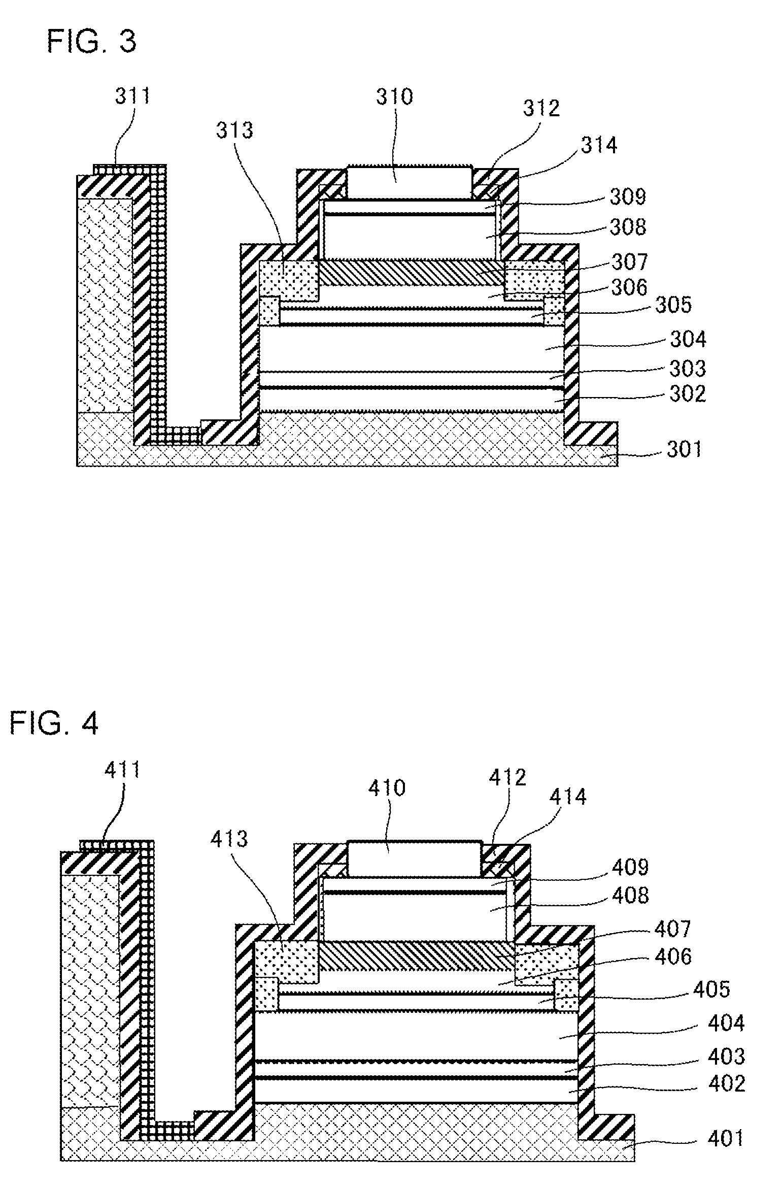
[0061]Configurations of second exemplary embodiment according to the present invention will be described in reference to FIG. 3. The semiconductor photo detector of second exemplary embodiment has a layer-structure, including a selective etching layer 302 of the first-type conductivity, a buffer layer 303 of the first-type conductivity, a multiplier layer 304 (undoped layer), a field-relaxing layer 305 of the second-type conductivity, a light absorption layer 306 of the second-type conductivity, a selective etching layer 307 of the second-type conductivity, a buffer layer 308 of the second-type conductivity, a contact layer 309 of the second-type conductivity, an electrode in the side of the second-type conductivity 310, which are sequentially deposited on a semiconductor substrate 301.

[0062]A second mesa is formed on the semiconductor substrate 301, and a first mesa is formed on the second mesa. The first mesa includes the buffer layer 308 of the second-type conductivity, the conta...

example 2

[0088]A configuration of a semiconductor photo detector in example 2 is shown in Table 2 and FIG. 4. A semiconductor photo detector of example 2 is configured that a control of electric field is conducted by utilizing a hydrogen passivation to enhance internal electric field and decrease electric field with the interface of the passivation.

TABLE 2IMPURITYTHICK-CONCEN-MATE-NESSTRATIONLAYERS AND NUMERALSRIAL(μm)(cm−3)SEMICONDUCTOR SUBSTRATE 401InPN-TYPE SELECTIVE ETCHINGInP0.21 × 1018LAYER 402N-TYPE BUFFER LAYER 403InAlAs0.11 × 1018MULTIPLIER LAYER 404InAlAs0.2UNDOPEDP-TYPE FIELD-RELAXING LAYERInAlAs0.15 × 1017405P-TYPE LIGHT ABSORPTIONInGaAs1.01 × 1016LAYER 406P-TYPE SELECTIVE ETCHINGInP0.25 × 1017LAYER 407P-TYPE BUFFER LAYER 408InAlAs0.61 × 1018P-TYPE CONTACT LAYER 409InGaAs0.25 × 1018

[0089]The semiconductor photo detector of example 2 is manufactured as follows. An n-type selective etching layer 402, an n-type buffer layer 403, a multiplier layer 404, a p-type field-relaxing layer ...

example 3

[0096]A configuration of a semiconductor photo detector in example 3 is shown in Table 3 and FIG. 5. A semiconductor photo detector of example 3 is configured to have a PIN-PD structure, in which a control of electric field is conducted by utilizing a hydrogen passivation to enhance internal electric field and decrease electric field with the interface of the passivation.

TABLE 3IMPURITYTHICK-CONCEN-MATE-NESSTRATIONLAYERS AND NUMERALSRIAL(μm)(cm−3)SEMICONDUCTOR SUBSTRATE 501InPN-TYPE SELECTIVE ETCHINGInP0.21 × 1018LAYER 502N-TYPE BUFFER LAYER 503InAlAs0.11 × 1018N-TYPE ELECTRONInAlAs1.01 × 1016TRANSPORT LAYER 504P-TYPE LIGHT ABSORPTIONInGaAs1.01 × 1016LAYER 506P-TYPE SELECTIVE ETCHINGInP0.25 × 1017LAYER 507P-TYPE BUFFER LAYER 508InAlAs0.61 × 1018P-TYPE CONTACT LAYER 509InGaAs0.25 × 1018

[0097]The semiconductor photo detector of example 3 is manufactured as follows. An n-type selective etching layer 502, an n-type buffer layer 503, an n-type electron transport layer 504, a p-type light...


PUM


Abstract

A semiconductor photo detector of the present invention includes a layer structure, having a selective etching layer of a first-type conductivity, a field-relaxing layer of the first-type conductivity, a multiplier layer, a field-relaxing layer of a second-type conductivity, a light absorption layer of the second-type conductivity, a selective etching layer of the second-type conductivity, a buffer layer of the second-type conductivity, a contact layer of the second-type conductivity, and an electrode in the side of the second-type conductivity, which are sequentially deposited over a semiconductor substrate, and having a second mesa formed on the semiconductor substrate and a first mesa formed on the second mesa, wherein the first mesa includes the buffer layer of the second-type conductivity, the contact layer of the second-type conductivity, and the electrode in the side of the second-type conductivity, wherein the second mesa includes the layer of the first-type conductivity, the multiplier layer, the light absorption layer of the second-type conductivity, and the selective etching layer of the second-type conductivity, wherein an outer periphery of the second mesa is located outside of the outer periphery of the first mesa in two-dimensional view, and wherein surfaces of the first mesa and the second mesa is covered by a passivation film.

Description

TECHNICAL FIELD[0001]The present invention relates to a semiconductor photo detector.BACKGROUND ART[0002]In various types of semiconductor photo detectors, p-i-n photodiode (hereinafter referred to as “PIN photodiode”) is well known. This device is capable of detecting photon as photoelectric current that is generated by the following processes, in which an electric field is applied over a low concentration layer of a semiconductor (I layer) sandwiched with a p-type layer and an n-type layer to generate photo carrier in the I layer, which travels therethrough to create photoelectric current.[0003]On the other hand, photo detectors exhibiting higher sensitivity are more useful in the field of optical communications and optical measurements. Devices referred to as avalanche photodiodes (hereinafter, abbreviated as “APD”), which utilize avalanche effect generated by applying strong electric field into a semiconductor, are often employed. A multiplier layer having higher internal electr...

Claims


Application Information

Patent Timeline
IPC IPC(8): H01L31/107H01L31/105
CPCH01L31/1075
Inventor NAKATA, TAKESHI
Owner NEC CORP
Learn More