

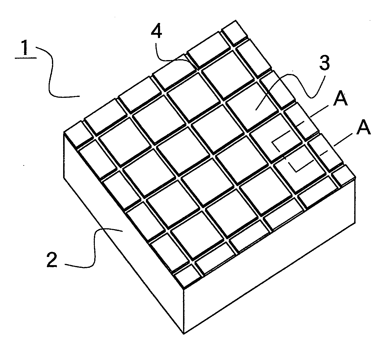
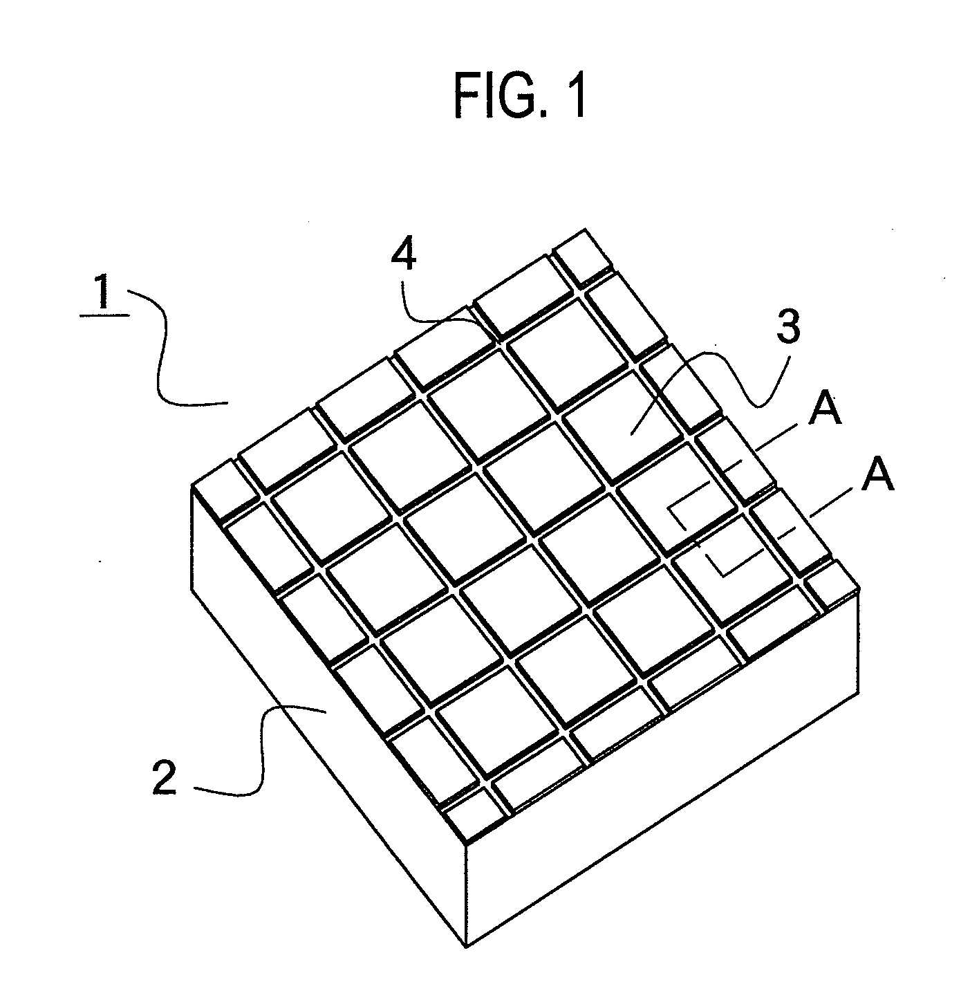
Engraved plate and substrate with conductor layer pattern using the same
a technology of conductor layer and engraved plate, which is applied in the field of engraving plate, can solve the problems of large number of manufacturing steps, inability to easily give accurate shape, and inability to obtain linearity of concave portion edge and concave portion thickness, so as to improve the adhesion of resist film used to form patterned insulating layer, improve the effect of surface smoothness and miniaturization of patterning
- Summary
- Abstract
- Description
- Claims
- Application Information
AI Technical Summary
Benefits of technology
Problems solved by technology
Method used
Image

Examples
example 1a
Formation of Convex Pattern
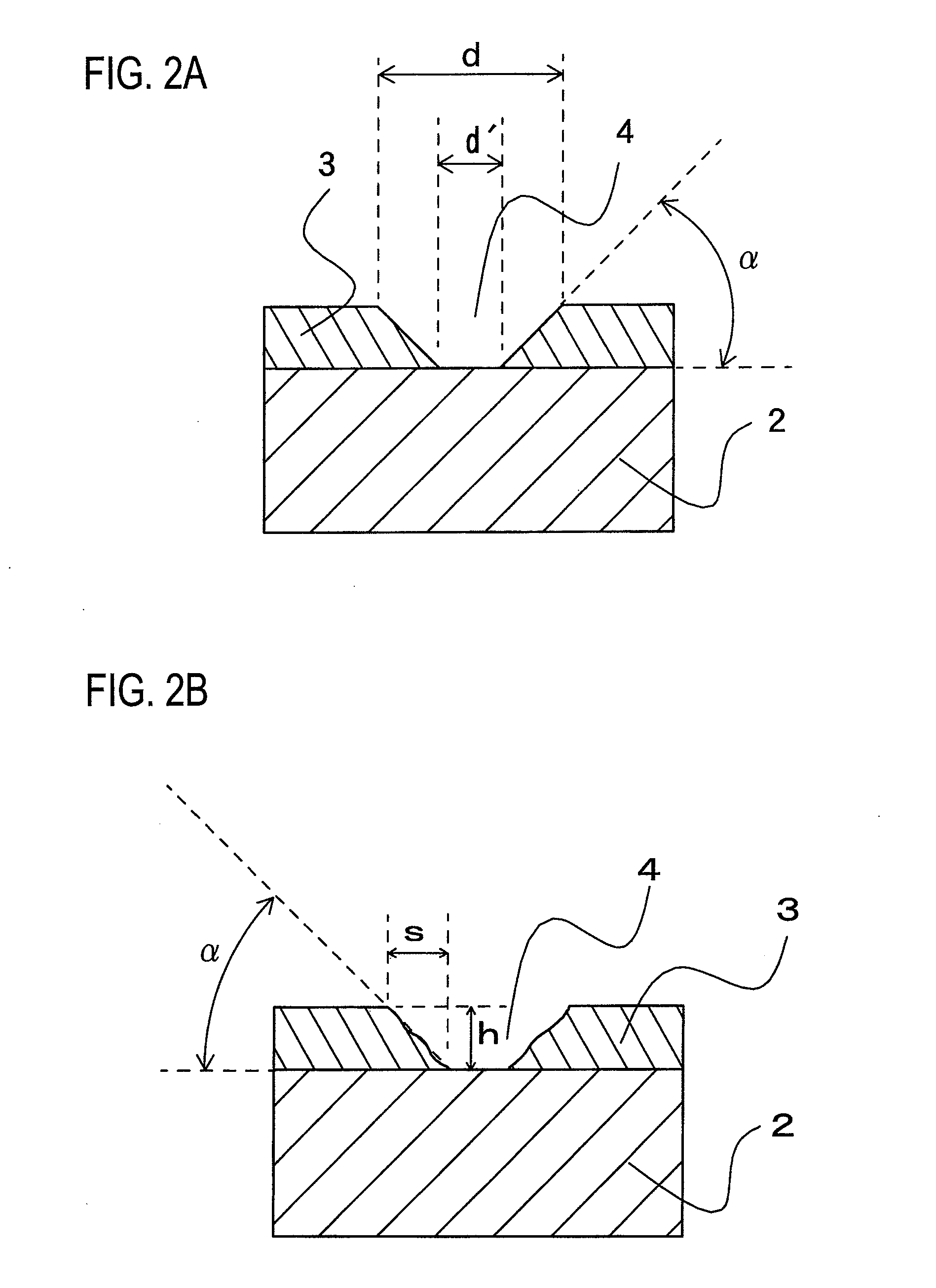
[0805]Resist films (PhoTec RY 3315, thickness: 10 μm (manufactured by Hitachi Chemical Co., Ltd.)) were laminated to both surfaces of a 150 mm square stainless steel plate (SUS316L, mirror finish, thickness: 300 μm, manufactured by NISSHIN STEEL CO., LTD.) (corresponding to FIG. 3A). As laminating conditions, a roll temperature was set to 105° C., a pressure was set to 0.5 MPa, and a line speed was set to 1 m / min. A negative film on which a lattice-shaped pattern of light-transmitting portion was formed at a line width of 15 μm and a line pitch of 300 μm in a 120 mm square area and at a bias angle of 45° (in the square area, lines are arranged at angle of 45° to the sides of the square area) was placed on one surface of the stainless steel plate at rest. By using an ultraviolet irradiation apparatus, under a degree of vacuum of 600 mmHg or less, ultraviolet rays were irradiated at 120 mJ / cm2 on the negative film for the upper and lower surfaces of the stai...
example 2a
Formation of Convex Pattern
[0822]A liquid resist (ZPN-2000, manufactured by ZEON CORPORATION) was applied to both the surfaces of a titanium plate of 150 mm square (pure titanium, mirror finish, a thickness of 400 μm, manufactured by Nippon Kinzoku co., Ltd.) The resist was coated three times to obtain a resist film having a thickness of 6 μm. After the resultant resist film was prebaked at 110° C. for 1 minute, a negative chromium mask on which a lattice-shaped pattern of light-transmitting portion was formed at a line width of 5 μm and a line pitch of 300 μm in a 110 mm square area and at a bias angle of 45° (in the square area, lines are arranged at angle of 45° to the sides of the square area) was placed on one surface of the titanium plate at rest. By using an ultraviolet irradiation apparatus, under a degree of vacuum of 600 mmHg or less, ultraviolet ray was irradiated at 200 mJ / cm2 for the upper surface of the titanium plate (as an adsorbed substrate) on which the chromium ma...
example 3a
[0836]A liquid resist (KMPR-1050, manufactured by NIPPON KAYAKU CO., LTD.) was applied to both the surfaces of a stainless steel substrate (SUS304, 314×150 mm, manufactured by NISSHIN STEEL CO., LTD.) to have a thickness of 15 μm. After the resultant resist film was prebaked at 90° C. for 10 minutes, two negative chromium masks on each of which a lattice-shaped pattern of light-transmitting portion was formed at a line width of 5 μm and a line pitch of 300 μm in a 110 mm square area and at a bias angle of 45° (in the square area, lines are arranged at angle of 45° to the sides of the square area) were placed on one surface of the stainless steel plate in parallel to each other at rest. By using an ultraviolet irradiation apparatus, under a degree of vacuum of 600 mmHg or less, an ultraviolet ray was irradiated at 200 mJ / cm2 for the upper surface of the stainless steel plate (as an adsorbed substrate) on which the chromium mask was placed. The ultraviolet ray was irradiated on the re...
PUM
| Property | Measurement | Unit |
|---|---|---|
| thickness | aaaaa | aaaaa |
| angle | aaaaa | aaaaa |
| angle | aaaaa | aaaaa |
Abstract
Description
Claims
Application Information