Process for producing surface emitting laser, process for producing surface emitting laser array, and optical apparatus including surface emitting laser array produced by the process

a surface emitting laser and laser array technology, which is applied in the direction of laser optical resonator construction, laser details, semiconductor lasers, etc., can solve the problems of low etching resistance and the inability to form a high-precision mesa structure, and achieve the effect of reducing the damage to the surface of the surface relief structur

Inactive Publication Date: 2010-02-04
CANON KK
View PDF31 Cites 17 Cited by
  • Summary
  • Abstract
  • Description
  • Claims
  • Application Information

AI Technical Summary

Benefits of technology

[0050]Thus, the inventors of the present invention found that, when the surface relief structure is protected by a second dielectric film 426 (see FIG. 5A

Problems solved by technology

Therefore, the etching resistance is low, and hence the m

Method used


Image

  • Process for producing surface emitting laser, process for producing surface emitting laser array, and optical apparatus including surface emitting laser array produced by the process
  • Process for producing surface emitting laser, process for producing surface emitting laser array, and optical apparatus including surface emitting laser array produced by the process
  • Process for producing surface emitting laser, process for producing surface emitting laser array, and optical apparatus including surface emitting laser array produced by the process

Examples


embodiments

Embodiment 1

[0063]In Embodiment 1, a process for producing a vertical cavity surface emitting laser having a convex surface relief structure is described.

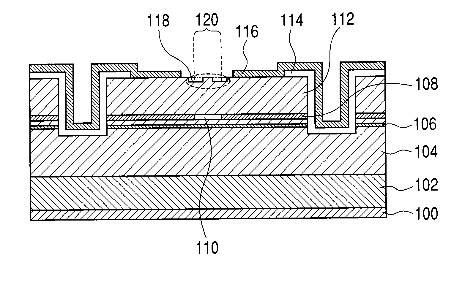
[0064]FIGS. 1A and 1B are schematic explanatory views illustrating a structure of the vertical cavity surface emitting laser in this embodiment.

[0065]FIG. 1A is a schematic cross sectional view illustrating the surface emitting laser in this embodiment. The surface emitting laser includes an n-side electrode 100, a substrate 102, a bottom distributed Bragg reflector (DBR) 104, an active layer 106, a current confinement portion (oxidized region) 108, and a non-oxidized region 110.

[0066]The surface emitting laser further includes atop DBR 112, an insulating film 114, a p-side electrode (pad electrode) 116, a surface relief structure 118, and a light output region 120.

[0067]FIG. 1B is an enlarged view illustrating the light output region 120 and the surroundings thereof. The light output region 120 includes a high-reflectance region 1...

embodiment 2

[0131]In Embodiment 2, a process for producing a vertical cavity surface emitting laser having a concave surface relief structure is described.

[0132]FIGS. 8A and 8B are schematic explanatory views illustrating a structure of the vertical cavity surface emitting laser in this embodiment.

[0133]FIG. 8A is a schematic explanatory cross sectional view illustrating a light output region 920. FIG. 8B is an enlarged view illustrating the light output region 920.

[0134]In FIGS. 8A and 8B, the same constituent elements as in Embodiment 1 illustrated in FIGS. 1A and 1B are expressed by the same reference numerals, and hence the duplicated descriptions are omitted.

[0135]In Embodiment 1, a high-reflectance region 922 is convex. In contrast, a low-reflectance region 924 is convex in this embodiment, and hence a concave surface relief structure is formed.

[0136]Next, the process for producing the surface emitting laser according to this embodiment is described.

[0137]A difference from the producing p...

embodiment 3

[0145]In Embodiment 3, a structural example of an optical apparatus using the vertical cavity surface emitting laser produced by the producing process according to any one of the embodiments described above is described.

[0146]A structural example of an image forming apparatus including a laser array using the surface emitting lasers is described as the optical apparatus.

[0147]FIGS. 10A and 10B are schematic explanatory views illustrating an electrophotographic recording type image forming apparatus in which the laser array using the vertical cavity surface emitting lasers is mounted, according to this embodiment.

[0148]FIG. 10A is a plan view illustrating the image forming apparatus and FIG. 10B is a side view illustrating the image forming apparatus. In FIGS. 10A and 10B, the image forming apparatus includes a photosensitive drum (photoreceptor) 1100, a charging unit 1102, a developing unit 1104, a transfer charging unit 1106, a fixing unit 1108, a rotatable polygon mirror 1110, and...


PUM


Abstract

Provided is a process for producing a surface emitting laser including a surface relief structure provided on laminated semiconductor layers, including the steps of transferring, to a first dielectric film, a first pattern for defining a mesa structure and a second pattern for defining the surface relief structure in the same process; and forming a second dielectric film on the first dielectric film and a surface of the laminated semiconductor layers to which the first pattern and the second pattern have been transferred. Accordingly, a center position of the surface relief structure can be aligned with a center position of a current confinement structure at high precision.

Description

BACKGROUND OF THE INVENTION[0001]1. Field of the Invention[0002]The present invention relates to a process for producing a surface emitting laser, a process for producing a surface emitting laser array, and an optical apparatus including the surface emitting laser array produced by the process.[0003]2. Description of the Related Art[0004]A vertical cavity surface emitting laser (hereinafter referred to as VCSEL) has been known as one of surface emitting lasers.[0005]In the surface emitting laser, an active region is sandwiched on both sides thereof by two reflectors to form a resonator in a direction perpendicular to a substrate, and light is emitted in the direction perpendicular to the substrate.[0006]It is important for the surface emitting laser to control transverse mode oscillation. When the surface emitting laser is to be applied to communications, a transverse mode output is required to be a single-mode output.[0007]Therefore, according to the surface emitting laser, a curre...

Claims


Application Information

Patent Timeline
IPC IPC(8): H01L21/00
CPCH01S5/18311H01S5/18369H01S2301/166H01S5/18391H01S5/423H01S5/18377H01S5/209H01S5/34326H01S5/10H01S5/183
Inventor UCHIDA, TATSUROIKUTA, MITSUHIROTAKEUCHI, TETSUYA
Owner CANON KK
Why Eureka
Try Eureka