

Manufacturing apparatus of composite substrate and manufacturing method of composite substrate with use of the manufacturing apparatus
a manufacturing apparatus and composite substrate technology, applied in the field of manufacturing apparatus of composite substrates, can solve the problems of semiconductor substrates moving on the base substrate, difficulty in relative alignment, and difficulty in bonding, and achieve the effects of improving alignment accuracy, reducing the amount of contaminants attached to the front surface of the second substrate, and high alignment accuracy
- Summary
- Abstract
- Description
- Claims
- Application Information
AI Technical Summary
Benefits of technology
Problems solved by technology
Method used
Image

Examples
embodiment 1
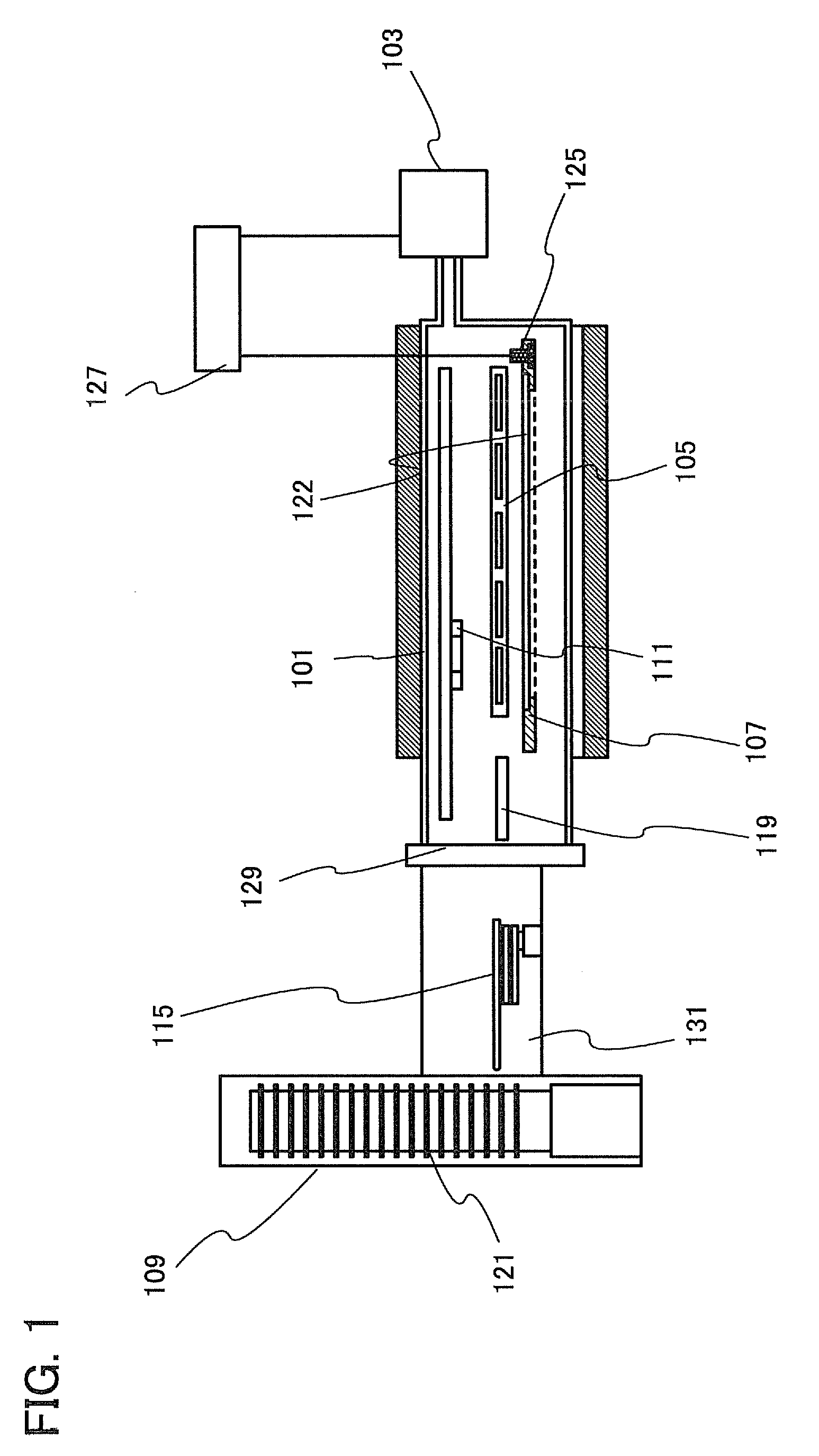
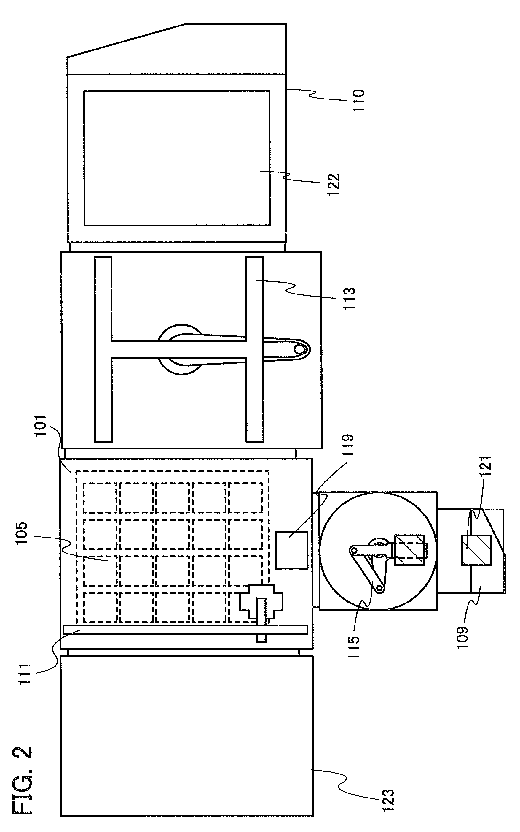
[0042]In this embodiment, a structure of a manufacturing apparatus of a composite substrate will be described with reference to drawings.
[0043]The manufacturing apparatus of a composite substrate illustrated in FIG. 1 and FIG. 2 includes a bonding chamber 101, a heat treatment means such as a heating gas supply unit 103, a first stage 105, a second stage 107, a first cassette chamber 109, a second cassette chamber 110, a first transfer means 111, a second transfer means 113, and a third transfer means 115.
[0044]In the bonding chamber 101, a first substrate 121 is bonded to a second substrate 122.
[0045]By the heat treatment means, heat treatment can be performed on the second substrate 122 and the first substrate 121 bonded to the second substrate 122. FIG. 1 illustrates an example in which the heating gas supply unit 103 is provided as the heat treatment means in the bonding chamber 101. In that case, it is preferable that the bonding chamber 101 have an inner wall made of quartz or...
embodiment 2
[0071]In this embodiment, an example of a manufacturing method of an SOI substrate, which uses the manufacturing apparatus of a composite substrate described in Embodiment 1, will be described with reference to drawings.
[0072]First, a plurality of semiconductor substrates corresponding to the first substrates 121 in Embodiment 1 are prepared. In this embodiment, a case of using a total of 20 semiconductor substrates of a semiconductor substrate 200a to a semiconductor substrate 200t will be described.
[0073]As the semiconductor substrates 200a to 200t, a commercial single crystal semiconductor substrate can be used. For example, it is possible to use a single crystal silicon substrate, a single crystal germanium substrate, or a compound semiconductor substrate of gallium arsenide, indium phosphide, or the like. A commercial silicon substrate typically has a circular shape with a size of 5 inches (125 mm) in diameter, 6 inches (150 mm) in diameter, 8 inches (200 mm) in diameter, or 12...
embodiment 3
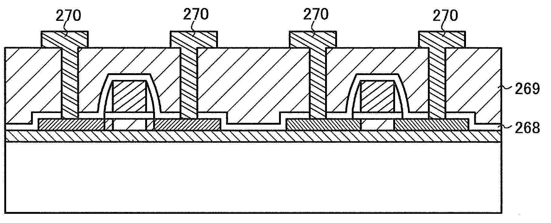
[0097]In this embodiment, a method for manufacturing a thin film transistor (TFT) using the aforementioned SOI substrate manufactured in Embodiment 2 will be described.
[0098]First, a method for manufacturing an n-channel thin film transistor and a p-channel thin film transistor will be described with reference to FIGS. 12A to 12D and FIGS. 13A to 13C. Various kinds of semiconductor devices can be formed by combining a plurality of thin film transistors (TFTs).
[0099]Description is made on the case where the SOI substrate manufactured by the method of Embodiment 2 is used as an SOI substrate.
[0100]FIG. 12A is a cross-sectional view of the SOI substrate manufactured by the method described with reference to FIG. 3.
[0101]The singe crystal semiconductor film 224a is patterned by etching to form semiconductor films 251 and 252 as illustrated in FIG. 12B. The semiconductor film 251 is included in an n-channel TFT, and the semiconductor film 252 is included in a p-channel TFT.
[0102]As illus...
PUM
| Property | Measurement | Unit |
|---|---|---|
| temperature | aaaaa | aaaaa |
| temperature | aaaaa | aaaaa |
| temperature | aaaaa | aaaaa |
Abstract
Description
Claims
Application Information