Superlens and lithography systems and methods using same

a superlense and lithography technology, applied in the field of plasmonic devices, can solve the problems of large wavelengths, difficult to achieve the effect of improving resolution, improving performance, and improving resolution

Inactive Publication Date: 2010-02-11
LEE HYESOG +2
View PDF11 Cites 32 Cited by
  • Summary
  • Abstract
  • Description
  • Claims
  • Application Information

AI Technical Summary

Benefits of technology

[0013]The novel design of certain embodiments discussed herein is facilitated by use of aluminum for the negative-index layer; use of an immersion layer between the aluminum and photoresist; use of photoresist material with resonant nanoparticles; and in one embodiment, use of multiple layers of aluminum separated by positive-index materials with different indices of refraction. Use of aluminum enables imaging of smaller features than currently obtainable via use of silver. The aluminum superlens may be used with 193-nanometer-wavelength electromagnetic energy to image features of a mask that are smaller than 100 nanometers at high resolutions, which is typically beyond conventional diffraction-limited resolutions. Furthermore, use of aluminum may result in improved performance over that of other metals, ...

Problems solved by technology

Unfortunately, such silver superlenses typically work with relatively large wavelengths of electromagnetic energy only, such as 365 nanometer-wavelengths.
Consequently, use of silver superlenses to image extremely small features, smaller than th...

Method used


Image

  • Superlens and lithography systems and methods using same
  • Superlens and lithography systems and methods using same
  • Superlens and lithography systems and methods using same

Examples


first embodiment

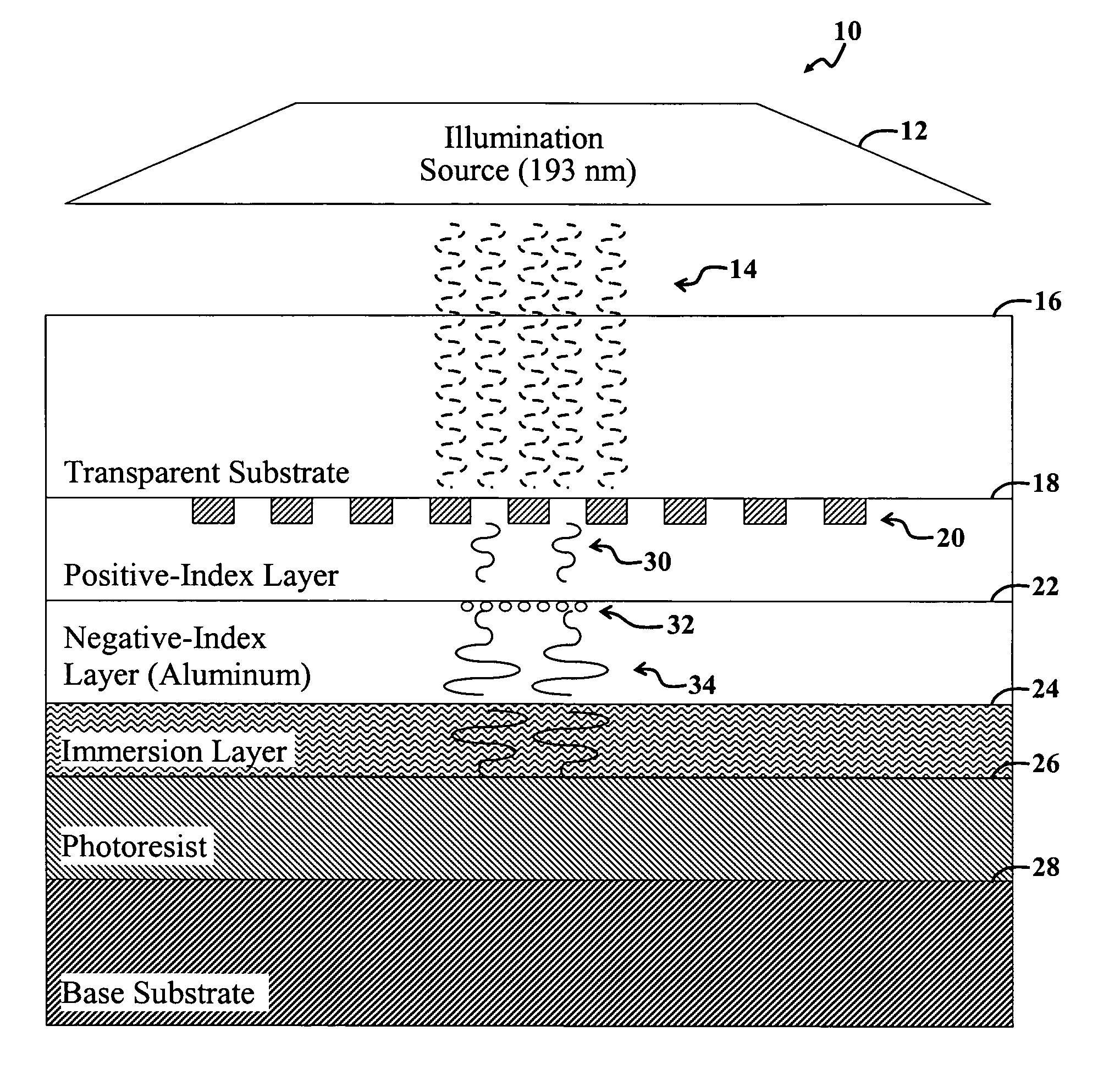
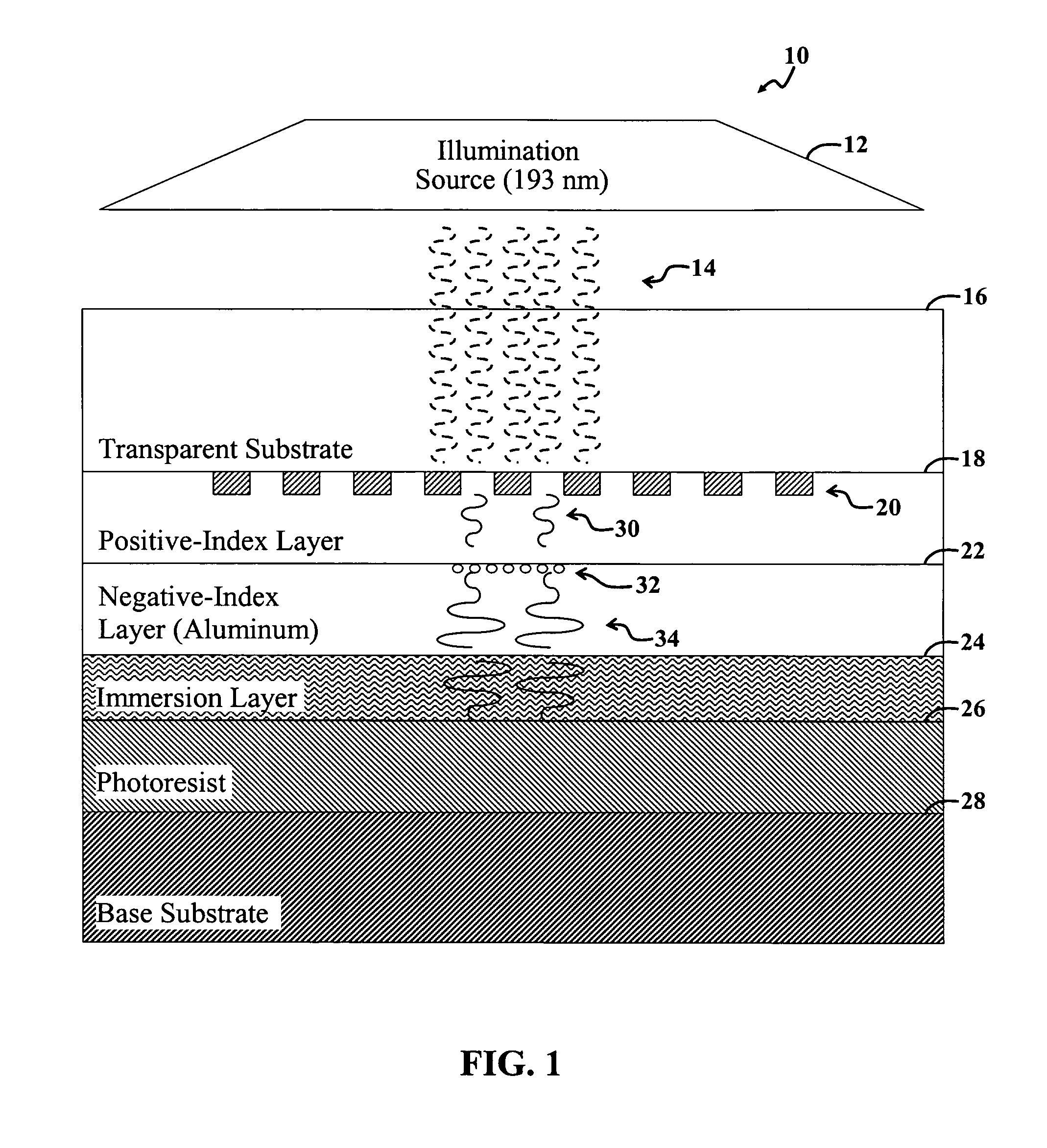
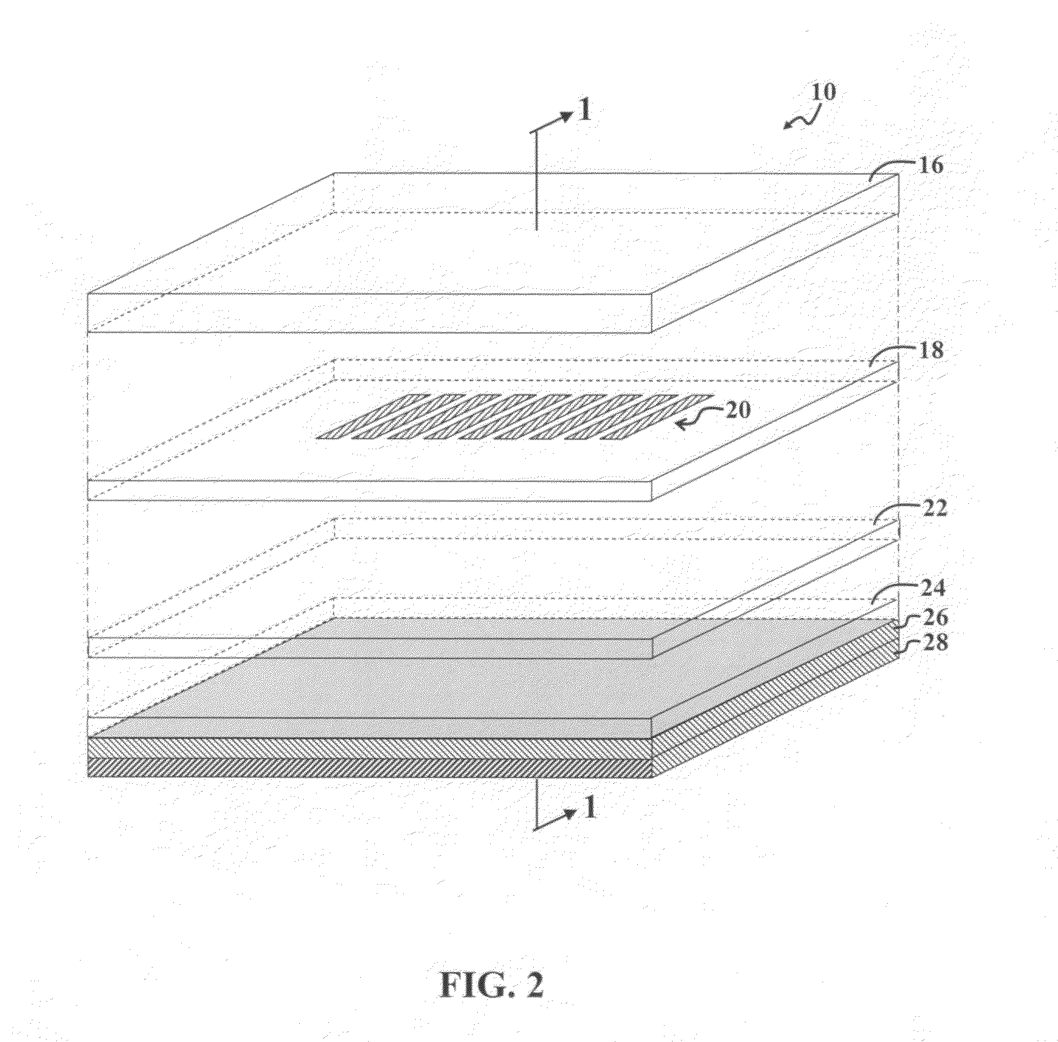
[0025]FIG. 1 is a diagram of a nanolithography system 10 for performing immersion lithography. For the purposes of the present discussion, a lithography system may be any device or collection of devices adapted to facilitate using an image or projection of an image, such as a mask pattern or other image, to create one or more physical features in or on a material. A nanolithography system may be any lithography system capable of facilitating the creation of nanometer-scale features. A nanometer-scale feature, also called a nanoscale feature, may be any feature or thing with one or more dimensions less than approximately 500 nanometers.

[0026]The present nanolithography system 10 is also called a superlens lithography system, or more specifically, a single-superlens nanolithography system, as it employs a single superlens to facilitate nanolithography. A superlens may be any lens or device capable of yielding an image characterized by a resolution less than the diffraction limit asso...

second embodiment

[0054]FIG. 3 is a diagram of a single-superlens nanolithography system 40 for performing contact lithography. The construction and operation of the second single-superlens lithography system 40 is similar to the construction and operation of the first super-lens lithography system 10 of FIG. 1 with the exception that the immersion layer 24 of FIG. 1 is removed in FIG. 2, and the mask 20 of FIG. 1 is replaced with a thicker mask 50 that extends into a transparent substrate 56 instead of extending into the positive-index layer 58. Furthermore, the illumination source 12 of FIG. 1 is replaced with the alternative illumination source 42, which is adapted to produce multiple selectively angled beams of collimated electromagnetic energy 46, 48. In the present specific embodiment, the beams 46, 48 are angled approximately forty-five degrees so that they intersect, forming an interference pattern 49. The interference pattern 49 represents a coupling of the beams 46, 48. By strategically co...

third embodiment

[0061]FIG. 4 is a diagram of a multi-superlens nanolithography system 60 for performing immersion lithography. The construction and operation of the multi-superlens nanolithography system 60 is similar to the construction and operation of the first single-superlens nanolithography system 10 of FIG. 1 with the exception that an additional superlens 62, 64 comprising a second positive-index layer 62 adjacent to a second negative-index layer 64 is positioned after the first negative-index layer 22 of the first superlens 18, 22. Furthermore, the mask 20 extends into a transparent substrate 66.

[0062]Evanescent waves output from the first negative-index layer 22 are slightly attenuated in the second positive-index layer 62 before being amplified again via surface plasmon resonance by the second negative-index layer 64. Use of multiple superlens as shown in FIG. 2 may further enhance resolution obtainable by the nanolithography system 60.

[0063]In the present specific embodiment, the secon...


PUM


Abstract

A superlens that includes, in one example embodiment, a positive-index material adjacent to a negative-index material, wherein the negative-index material includes aluminum. In a more specific embodiment, the positive-index material includes a dielectric layer, such as Poly(Methyl MethAcrylate) (PMMA), which is less than 50 nanometers thick. The negative-index material includes a smoothed aluminum layer less than 50 nanometers thick. The aluminum layer is disposed on the dielectric layer or vice versa, forming a superlens comprising the aluminum layer and the dielectric layer. In another embodiment, the superlens further includes plural aluminum layers separated by one or more layers of positive-index material. A mask is adjacent to the positive-index material. The mask may include one or more features that extend into a transparent substrate. The mask is positioned so that the positive-index material separates the mask from the smoothed aluminum layer. In an illustrative embodiment, the superlens is adapted for use with thermal lithography using nanoparticles.

Description

BACKGROUND OF THE INVENTION[0001]1. Field of Invention[0002]This invention relates to plasmonic devices. Specifically, the present invention relates to imaging devices, systems, and methods that use electromagnetic energy and plasmons.[0003]2. Description of the Related Art[0004]Plasmonic superlenses may be employed in various demanding applications, including nanolithography for fabricating high-density integrated circuits and extremely small electromechanical devices. Such applications demand cost-effective superlenses and accompanying lithography methods that can reliably be used to create nanometer-scale features.[0005]For the purposes of the present discussion, nanolithography may be any method that uses an imaging system or device to create physical features or things that are characterized by one or more dimensions less than approximately 500 nanometers. A feature or thing with dimensions less than approximately 500 nanometers is called a nanoscale feature. An imaging system ...

Claims


Application Information

Patent Timeline
IPC IPC(8): G03B27/54G03B27/32
CPCG03F1/14G03F1/54G03F7/70341G03F7/70325G03F7/2014G03F1/50
Inventor LEE, HYESOGSIVILOTTI, MASSIMO A.VERMA, RAVI K.
Owner LEE HYESOG
Why Eureka
Try Eureka