Process For Through Silicon Via Filing

a technology of silicon vias and filing processes, which is applied in the direction of electrolysis components, electric circuits, manufacturing tools, etc., can solve the problems of difficult depositing of copper into such structures, limited step coverage, and high cost of precursors, and achieves fast copper migration, high aspect ratio, and large size

Active Publication Date: 2010-02-18
NOVELLUS SYSTEMS
View PDF6 Cites 61 Cited by
  • Summary
  • Abstract
  • Description
  • Claims
  • Application Information

AI Technical Summary

Benefits of technology

[0007]The present invention provides copper electroplating methods and associated apparatus for electroplating copper in through silicon via (TSV) holes having large sizes and high aspect ratios. The plating solution for copper deposition inside the TSV holes may have a relatively low concentration of sulfuric acid and high concentration of copper ions. TSV deposition processes may benefit from faster copper migration through the plating solution and, in particular, to the bottom of the T

Problems solved by technology

TSV holes typically have high aspect ratios and depositing copper into such structures can be challenging.
CVD deposition of copper requires complex and expensive precursors, while PVD deposition often results in voids and limited step coverage.
Electroplating is a more common method of depositing copper into TSV struct

Method used


Image

  • Process For Through Silicon Via Filing
  • Process For Through Silicon Via Filing
  • Process For Through Silicon Via Filing

Examples


Embodiment Construction

[0025]In the following description, numerous specific details are set forth in order to provide a thorough understanding of the present invention. The present invention may be practiced without some or all of these specific details. In some instances, well known process operations have not been described in detail to not unnecessarily obscure the present invention. While the invention will be described in conjunction with the specific embodiments, it will be understood that it is not intended to limit the invention to the embodiments.

[0026]In this disclosure various terms are used to describe a semiconductor processing work piece. For example, “wafer” and “substrate” are used interchangeably. The process of depositing, or plating, metal onto a conductive surface via an electrochemical reaction is referred to generally as electroplating or electrofilling.

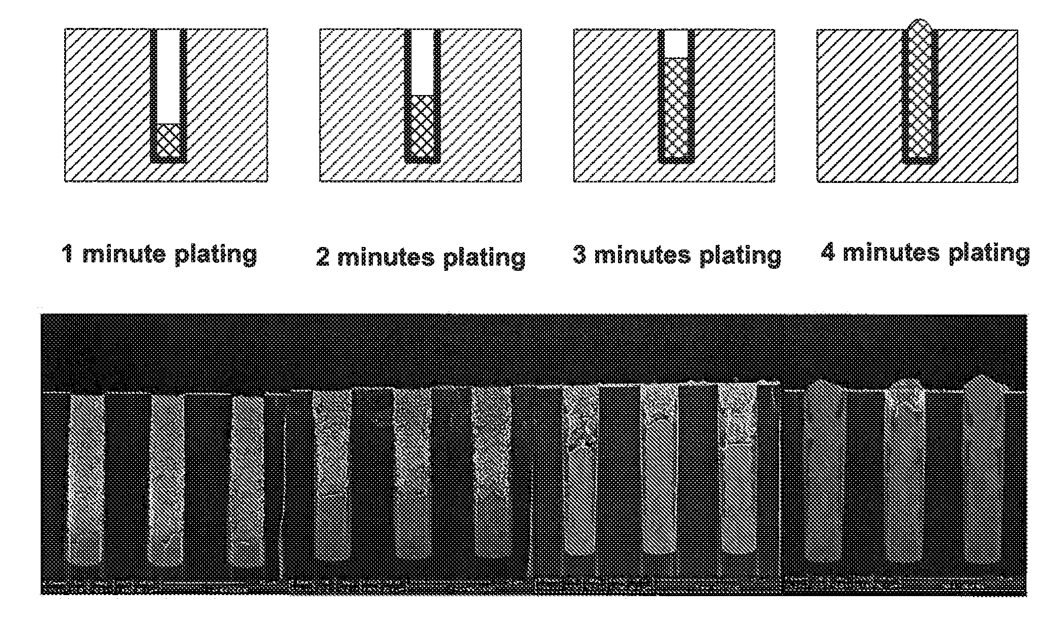
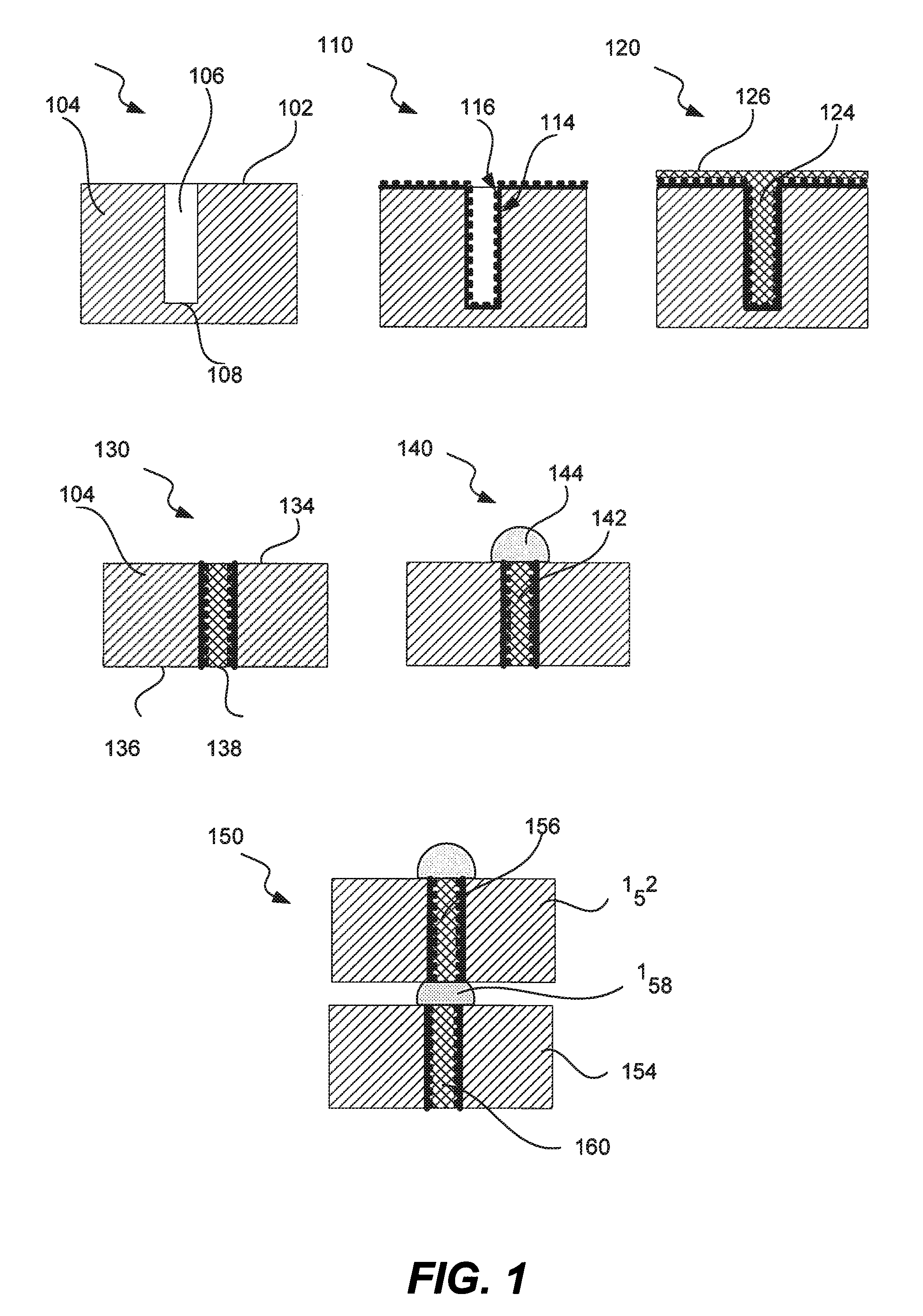
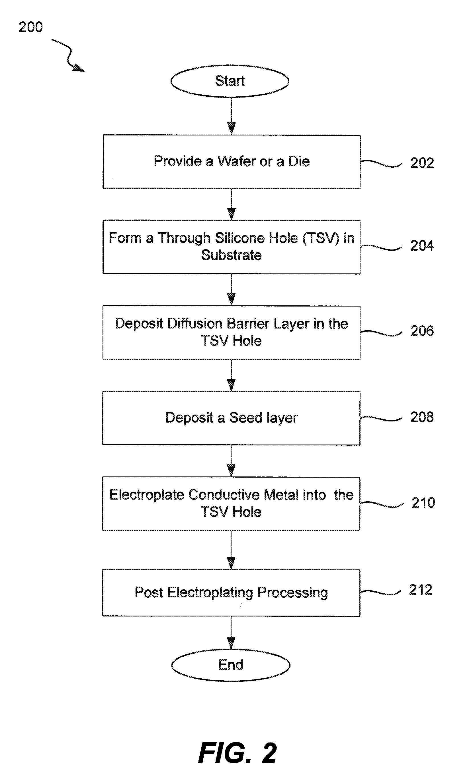
Through Silicon Vias

[0027]A through-silicon via (TSV) is a vertical electrical connection passing completely through a silicon wafe...


PUM

PropertyMeasurementUnit
Temperatureaaaaaaaaaa

Abstract

A semiconductor electroplating process deposits copper into the through silicon via hole to completely fill the through silicon via in a substantially void free is disclosed. The through silicon via may be more than about 3 micrometers in diameter and more that about 20 micrometers deep. Low copper concentration and high acidity electroplating solution is used for deposition copper into the through silicon vias.

Description

FIELD OF THE INVENTION[0001]The present invention relates generally to methods and apparatus for depositing copper onto a wafer and more particularly to methods and apparatus for electroplating copper into through silicon vias having relatively large sizes and high aspect ratios that may interconnect stacked electronic devices.BACKGROUND OF THE INVENTION[0002]A through-silicon via (TSV) is a vertical electrical connection passing completely through a silicon wafer or die. TSV technology is important in creating 3D packages and 3D integrated circuits (IC). It provides interconnection of vertically aligned electronic devices through internal wiring that significantly reduces complexity and overall dimensions of a multi-chip electronic circuit.[0003]A typical TSV process includes formation of TSV holes and deposition of a diffusion barrier layer and a conductive seed layer. A conductive material is then electroplated into TSV holes. Copper is typically used as the conductive material a...

Claims


Application Information

Patent Timeline
IPC IPC(8): H01L21/445C25D3/38C25D17/00
CPCC25D3/38C25D21/12H01L21/2885H01L21/76898H01L2224/16H01L2225/06513H01L2225/06541C25D7/123C25D17/001H01L25/50H01L2224/0554H01L2224/05573H01L2224/13025H01L2924/00014H01L2224/05599H01L2224/0555H01L2224/0556
Inventor REID, JONATHAN D.WANG, KATIE QUNWILLEY, MARK J.
Owner NOVELLUS SYSTEMS
Why Eureka
Try Eureka