Hybrid metal-semiconductor nanoparticles and methods for photo-inducing charge separation and applications thereof

a technology of metal-semiconductor nanoparticles and photo-inducing charge separation, which is applied in the direction of nanoinformatics, energy input, physical/chemical process catalysts, etc., can solve the problems of limited photocatalytic activity efficiency, limited examples of semiconductor-metal systems for photocatalysis, and severe limitations of semiconductor-metal applications of photocatalysts, etc., to achieve efficient utilization of the whole range of wavelengths, improve control

Inactive Publication Date: 2010-02-25
YISSUM RES DEV CO OF THE HEBREWUNIVERSITY OF JERUSALEM LTD
View PDF6 Cites 41 Cited by
  • Summary
  • Abstract
  • Description
  • Claims
  • Application Information

AI Technical Summary

Benefits of technology

[0103]In addition, nanoparticle populations comprising any one nanoparticle according to the invention or employed in any one method of the invention, and at least one type of particle outside of the scope of the present application are also provided herein. Such mixed populations of nanoparticles herein described and nanoparticles known in the art may have advantageous effects suitable for any one application disclosed herein.
[0104]As will be discussed further below, by having the ability to provide blends of different nanoparticle populations it is possible to tune the optical properties of the material, thus utilizing the whole range of wavelengths efficiently. Alternations in the metal composition and size allow the fine-tuning of the Fermi level energy and the redox potential of the nanostructure. The different shapes enable better control and the design of a great variety of devices.
[0105]As will be further shown below, the nanoparticle populations of the invention may form a net-like arrangement, herein referred to as “nanonets”, with the individual nanoparticles strongly interacting with each other to create a single net-like structure as shown, for example, in FIGS. 11b, 11c and 11d. In the nanonet structure, the semiconductor segments are fused with covalent binding, resulting in strong coupling between the segments and the surface is decorated with metal islands.
[0106]It is emphasized that the nanonet structure results in a structure that is by no means a mere random aggregation or collection of nanoparticles. Such a random aggregation or collection is typically characterized as having an overall low surface area resulting from the blocking (partially or wholly) of the surface area of the individual nanoparticles due to the three-dimensional structure of the random aggregate. Such aggregates are less stable and decompose under less stringent conditions to smaller aggregates or to the individual nanoparticles.
[0107]Unlike a random aggregation or collection of nanoparticles, the nanonet structures of the invention are more porous, having a more exposed high surface area structure composed of interconnecting (fused) nanostructures. In fact, when nanonets of the invention are inspected it is nearly impossible to distinguish the contact points between the original nanoparticles, e.g., nanorods or spherical-like particles that were used to prepare this structure.
[0108]As experiments have shown, in typical aggregates, the photocatalytic activity may be reduced or quenched. The nanonets of the invention exhibit photocatalysis activity and are in a form that is desirable for a photocatalyst since they can easily become stationary on a substrate or membrane structure and could easily be separated from a photocatalysis reaction solution.

Problems solved by technology

However, due to the rapid recombination of charge carriers in the semiconductor itself, the efficiency of the photocatalytic activity is limited as the charge carriers are not labile for redox reactions.
Thus far, examples of semiconductor-metal systems for photocatalysis were limited in several aspects; First, most semiconductor photocatalysts were based on high-band gap semiconductors such as TiO2, ZnO and CdS [11,12,13,14].
The high band gap semiconductor limits severely the applicability of the photocatalyst, as it does not match the solar spectrum.
Even in the case of Bao et al [6], who reported the production of Pt-loaded CdS nanostructures for photocatalytic production of hydrogen under blue light, the band gap of the CdSe nanostructure was limited to wavelengths of 520 nm and below, which limits the range of solar absorption of the photocatalyst.
Moreover, only limited control of nanostructure size and shape was achieved and the metal deposition was also with limited control.
Second, all of the systems developed thus far are not well controlled in terms of the metal islands size, location of the metal on the semiconductor and even in metal type.
In fact, the combined semiconductor-metal systems suffer from broad size, shape and even composition distributions.
This limits not only the ability to research and understand the performance of the photocatalyst but also the ability to improve it in a controlled manner.
These structures reduced the chemical processability of the nanoparticles, their homogenous distribution in a liquid / gel medium and their sophisticated use in more complex structures (such as a homogenous self-assembled thin film, or coating of an electrode surface) without altering their properties.

Method used


Image

  • Hybrid metal-semiconductor nanoparticles and methods for photo-inducing charge separation and applications thereof
  • Hybrid metal-semiconductor nanoparticles and methods for photo-inducing charge separation and applications thereof
  • Hybrid metal-semiconductor nanoparticles and methods for photo-inducing charge separation and applications thereof

Examples


Embodiment Construction

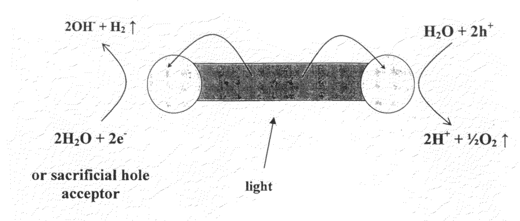
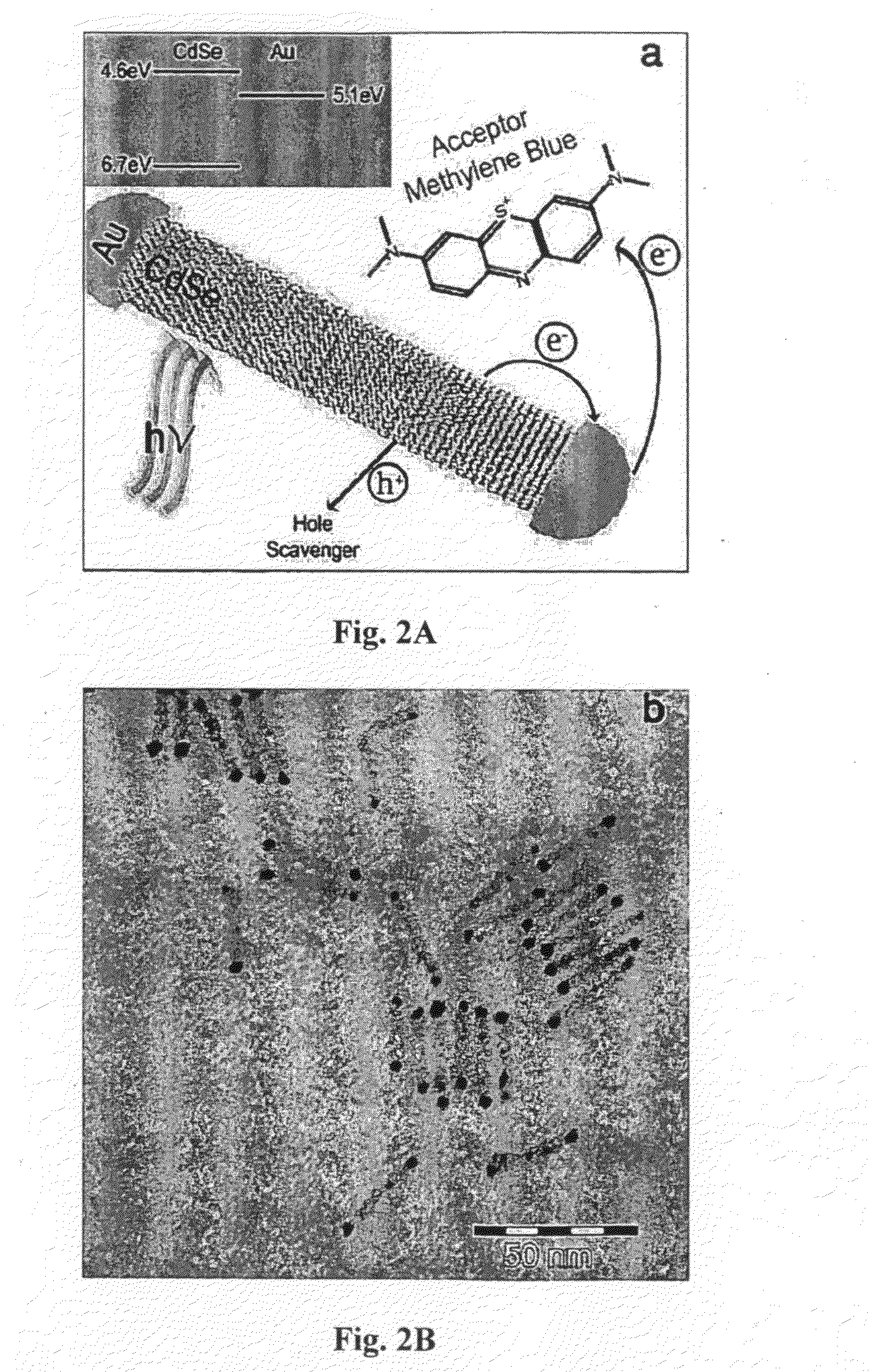
[0193]Visible light photocatalysis is a promising route for converting solar energy to chemical energy. Semiconductors and metal-semiconductor hybrid materials have been studied as photocatalysts in photochemical water-splitting to produce hydrogen, in photoelectrochemical cells and in photochemical purification of organic contaminants and bacterial detoxification. So far, semiconductor / metal hybrid photocatalysts were based mostly on wide-gap semiconductors limiting their applicability to the UV range, which consists of less than 5% of the solar spectrum. Additionally, they were poorly controlled in terms of the semiconductor particle and metal island size, shape and location thus limiting their understanding and controlled improvement.

[0194]The inventors of the present invention demonstrate the visible range photocatalytic activity of highly controllable hybrid gold tipped CdSe nanorods, herein termed nanodumbbells (NDBs). As stated above, following light absorption, rapid charge ...


PUM

PropertyMeasurementUnit
wavelengthsaaaaaaaaaa
lengthaaaaaaaaaa
lengthaaaaaaaaaa

Abstract

The development and use of hybrid metal-semiconductor nanoparticles for photocatalysis of a variety of chemical reactions such as redox reactions and water-splitting, is provided.

Description

FIELD OF THE INVENTION[0001]This invention relates generally to hybrid metal-semiconductor nanoparticles, uses thereof in photo-induced charge separation reactions and applications.BACKGROUND OF THE INVENTION[0002]Photocatalysis is the acceleration of a photoreaction in the presence of a catalyst. In photo-generated catalysis the photocatalytic activity depends on the ability of a catalyst to absorb light and create electron-hole pairs, which can later enable secondary reduction-oxidation (redox) reactions.[0003]A landmark in photocatalysis is the discovery of water electrolysis by means of a light induced process on titanium dioxide (termed ‘photocatalytic water splitting’) [1]. Photocatalysis has important commercial applications in water splitting and in additional areas including water and air purification, degradation of organic contaminants such as residues from the dye industry [2] and in photoelectrochemical cells [3]. An interesting and promising aspect of this technology i...

Claims


Application Information

Patent Timeline
Patent Type & Authority Applications(United States)
IPC IPC(8): C01B3/04
CPCB01J27/0573B01J35/004B82Y30/00C01B3/042C25B1/003H01G9/20H01L51/4266Y02E60/364H01B1/16Y02E60/36Y02P20/133C25B1/55Y02E10/50H10K30/352B82B1/00B01J35/00H01L31/04B82Y10/00
Inventor BANIN, URICOSTI, RONNY
Owner YISSUM RES DEV CO OF THE HEBREWUNIVERSITY OF JERUSALEM LTD
Why Eureka
Try Eureka