Semiconductor device, display device, and electronic device

a technology of semiconductor elements and display devices, applied in semiconductor devices, semiconductor/solid-state device details, instruments, etc., can solve the problems of difficulty in marking letters on the back surface of semiconductor elements at a size, limited number of letters contained in a mark code, and difficulty in reading the mark for confirmation and management of components, etc., to achieve easy readable and well-known, large mark formation area, and easy readable

Inactive Publication Date: 2010-02-25
SHARP KK
View PDF3 Cites 3 Cited by
  • Summary
  • Abstract
  • Description
  • Claims
  • Application Information

AI Technical Summary

Benefits of technology

[0030]In a semiconductor device according to the present invention, an interposer to which a semiconductor is connected has a larger area than that of the semiconductor. Hence, it is possible to attain a larger mark formation region. By displaying relatively large sized letters, it is possible to form a mark that is easily readable and well recognized. Moreover, limitation in the number of letters that can be marked is also relaxed. Thus, a code system which has good traceability containing enough amount of information to trace a manufacturing history can be easily applied.
[0031]Furthermore, a semiconductor device component which has a mark that is well recognized and has traceability that enables easy tracing of component history can be used in an electronic device such as a display device and the like which include the semiconductor device according to the present invention. Hence, it is possible to improve work reliability in a component assembling step, while also facilitating quality management of the product.

Problems solved by technology

Because of this, it is becoming difficult to mark letters on the back surface of the semiconductor element at a size easily recognizable by the naked eye or a machine.
Hence, hindrance occurs in reading the mark for confirmation and management of components, in an assembling step of a product that uses, as a component, the semiconductor device including the semiconductor element.
However, the number of letters contained in a mark code is limited due to the limit of the marking area.
Thus, a sufficient code system cannot be implemented.
Thus, such difficulty in recognition of the mark and insufficient traceability in the semiconductor device of such modes may cause effect to reliability of the product of the display device.

Method used


Image

  • Semiconductor device, display device, and electronic device
  • Semiconductor device, display device, and electronic device
  • Semiconductor device, display device, and electronic device

Examples


first embodiment

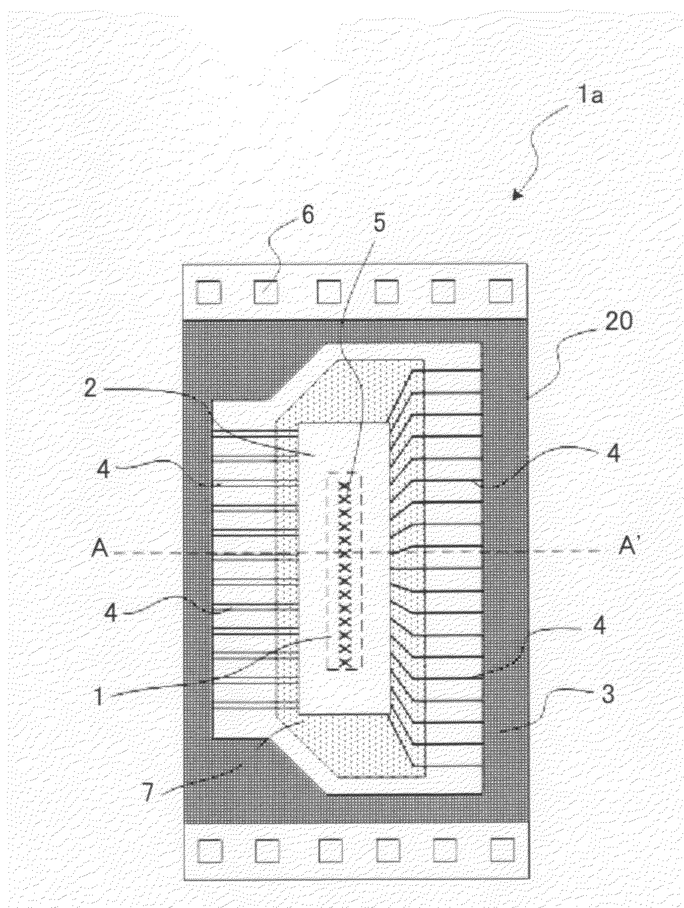
[0046]FIG. 1 is a plan view illustrating a liquid crystal driver mounting package, which is one embodiment of a semiconductor device according to the present invention.

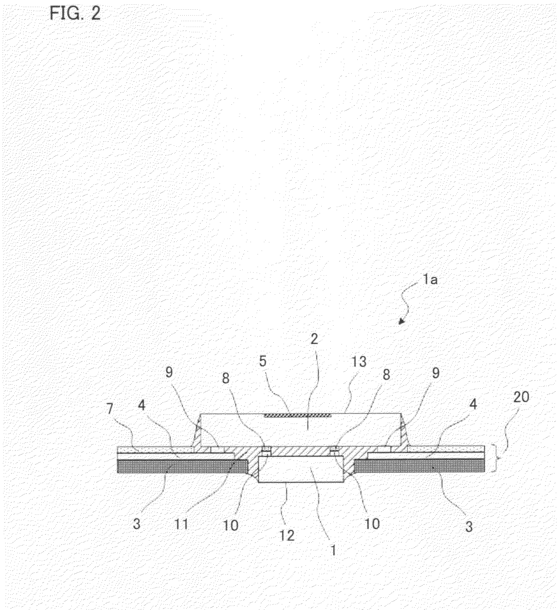
[0047]A liquid crystal driver mounting package 1a of the present embodiment is a COF type package in which a semiconductor element (liquid crystal driver) 1 is electrically connected to a circuit board (tape carrier) 20 via an interposer 2. In FIG. 1, the liquid crystal driver 1 is provided on a back surface of the interposer 2. Thus, a position of the liquid crystal driver 1 which actually cannot be seen is shown by a dotted line.

[0048]A part illustrated in FIG. 1 is one unit of a long tape carrier, which one unit constructs one package. The tape has sprocket holes 6 on both side sections of the tape, for transferring this long tape. The tape carrier is constructed of a film material 3 whose main component is polyimide, wiring pattern 4 made of copper foil and provided on one side of the film material 3, and resist r...

second embodiment

[0076]FIG. 5 illustrates an example of a mounting body of a BGA (Ball Grid Array) type in which a semiconductor element is mounted, as another example of a semiconductor device according to the present invention. Note that any arrangements which have the same function as the arrangements in the liquid crystal driver mounting package described before has the same reference sign attached thereto, and duplicating explanations will be omitted.

[0077]A semiconductor element (IC chip) 81 is interconnected with the interposer 2 by flip chip bonding, and furthermore, the interposer 2 is connected to a wiring pattern 4 provided on a circuit board 90, so as to be mounted in a BGA-type mounting body 1b.

[0078]The circuit board 90 is made of insulating material 83 such as glass epoxy resin or ceramic. The wiring pattern 4 provided on the insulating material 83 is connected to solder bumps 85 formed in a gridlike sequence on a reverse side of the insulating material 83, via respective via holes 8...


PUM


Abstract

In order to attain, in a semiconductor device in which a semiconductor element is mounted, formation of a mark of a relatively large size which is easily recognizable by the naked eye or a machine, and which can apply a code system containing enough amount of information for tracing a manufacturing history, a semiconductor device according to the present invention includes an interposer electrically connected to a semiconductor element, which semiconductor device has a mark for displaying at least predetermined information relevant to the semiconductor element.

Description

TECHNICAL FIELD[0001]The present invention relates to a semiconductor device in which a semiconductor element reduced in size is mounted, and a display device and an electronic device each of which includes the semiconductor device.BACKGROUND ART[0002]A liquid crystal display device has been adopted in various devices such as a television, a monitor for a personal computer, and a mobile phone. Due to an increase in the amount of information that is required to be displayed, in the recent years, achievement of high-definition and high-performance have been advanced for the liquid crystal display device. Accordingly, further multi output has been requested from a liquid crystal driver which is a semiconductor element to be provided in the liquid crystal display device. In response to this, reduction in size of a driver circuit, fine pitching of a bump provided on a chip of the semiconductor element, and the like have been carried out so as to attain further multi output by the liquid ...

Claims


Application Information

Patent Timeline
Patent Type & Authority Applications(United States)
IPC IPC(8): H01L23/48
CPCG02F1/13452H01L21/6836H01L2224/2919H01L2924/00013H01L2924/19105H01L2924/1532H01L2924/15311H01L23/4985H01L23/544H01L24/81H01L24/83H01L2221/68327H01L2223/54433H01L2223/54473H01L2223/5448H01L2223/54486H01L2224/13144H01L2224/16H01L2224/81203H01L2224/81801H01L2224/83851H01L2924/01079H01L2924/09701H01L2924/00014H01L2224/13099H01L2924/00011H01L2224/0401
Inventor KATOH, TATSUYAKUDOSE, SATORUNAKAGAWA, TOMOKATSU
Owner SHARP KK
Why Eureka
Try Eureka