
Method for forming nitride semiconductor laminated structure and method for manufacturing nitride semiconductor element

a technology of nitride and laminated structure, which is applied in the direction of semiconductor devices, electrical apparatus, transistors, etc., can solve the problems of not being able to implement a normally-off operation, which can be regarded as indispensable for a power device, and achieve the effect of increasing the resistance of the p-type gan layer

Active Publication Date: 2010-02-25
ROHM CO LTD
View PDF10 Cites 16 Cited by
  • Summary
  • Abstract
  • Description
  • Claims
  • Application Information

AI Technical Summary

Benefits of technology

[0008]In the aforementioned manufacturing method, however, H2 may be mixed into the p-type GaN layer when the p-type GaN layer is laminated, to be bonded to Mg in the p-type GaN layer. When an H—Mg bond is formed, Mg in the p-type GaN layer is inactivated and does not function as an acceptor, and the resistance of the p-type GaN layer may be increased.
[0013]According to the method, the n-type or i-type first layer is formed, and the p-type second layer containing Mg is formed on the first layer. After the second layer is formed, the n-type or i-type third layer is formed on the second layer while no activation annealing treatment is performed on the second layer. Thus, the nitride semiconductor laminated structure is so formed as to hold the p-type second layer between the n-type or i-type first and third layers, whereby Mg in the second layer of the laminated structure can be kept in an active state to function as an acceptor. Consequently, the resistance of the second layer can be reduced, whereby the nitride semiconductor laminated structure can be suitably employed as a semiconductor structure of a power device requiring a high current. Further, no activation annealing treatment is required, whereby mass productivity is improved.
[0018]Thus, a normally-off operation, i.e., an operation for setting an OFF-state between the source and the drain when applying no bias to the gate electrode can be easily implemented due to the basic structure as the vertical MISFET. Further, a high current can be easily fed, and high withstand voltage characteristics can also be easily ensured by increasing the thickness of the first layer. Therefore, an effective power device can be provided. Needless to say, the MISFET is constituted of the group III nitride semiconductors, whereby the same can attain characteristics such as a high withstand voltage, a high-temperature operation, a high current density, high-speed switching and small on-resistance as compared with a device employing a silicon semiconductor. In particular, the MISFET is capable of an operation with a high withstand voltage and low loss, whereby an excellent power device can be implemented.
[0024]Thus, the region where the inversion layer (the channel) is formed becomes the fourth layer in the aforementioned operation of the MISFET. Therefore, when the fourth layer is composed of a p-type semiconductor having an acceptor concentration lower than the acceptor concentration (the Mg concentration) of the second layer, for example, a gate voltage value necessary for forming the inversion layer can be suppressed lower as compared with a case where the conductivity of the region where the inversion layer is formed is identical to the conductivity of the second layer. The main factor deciding the voltage value of reach-through breakdown is the acceptor concentration of the overall second layer, and hence the gate threshold voltage can be reduced while ensuring high withstand voltage characteristics of the transistor as a result, and an excellent power device can be implemented.

Problems solved by technology

Therefore, such a GaN device is not necessarily suitable for a power device requiring a high current, and there is such a problem that implementation of a normally-off operation which can be regarded as indispensable for a power device is not necessarily easy.

Method used


Image

  • Method for forming nitride semiconductor laminated structure and method for manufacturing nitride semiconductor element
  • Method for forming nitride semiconductor laminated structure and method for manufacturing nitride semiconductor element
  • Method for forming nitride semiconductor laminated structure and method for manufacturing nitride semiconductor element

Examples


example 1

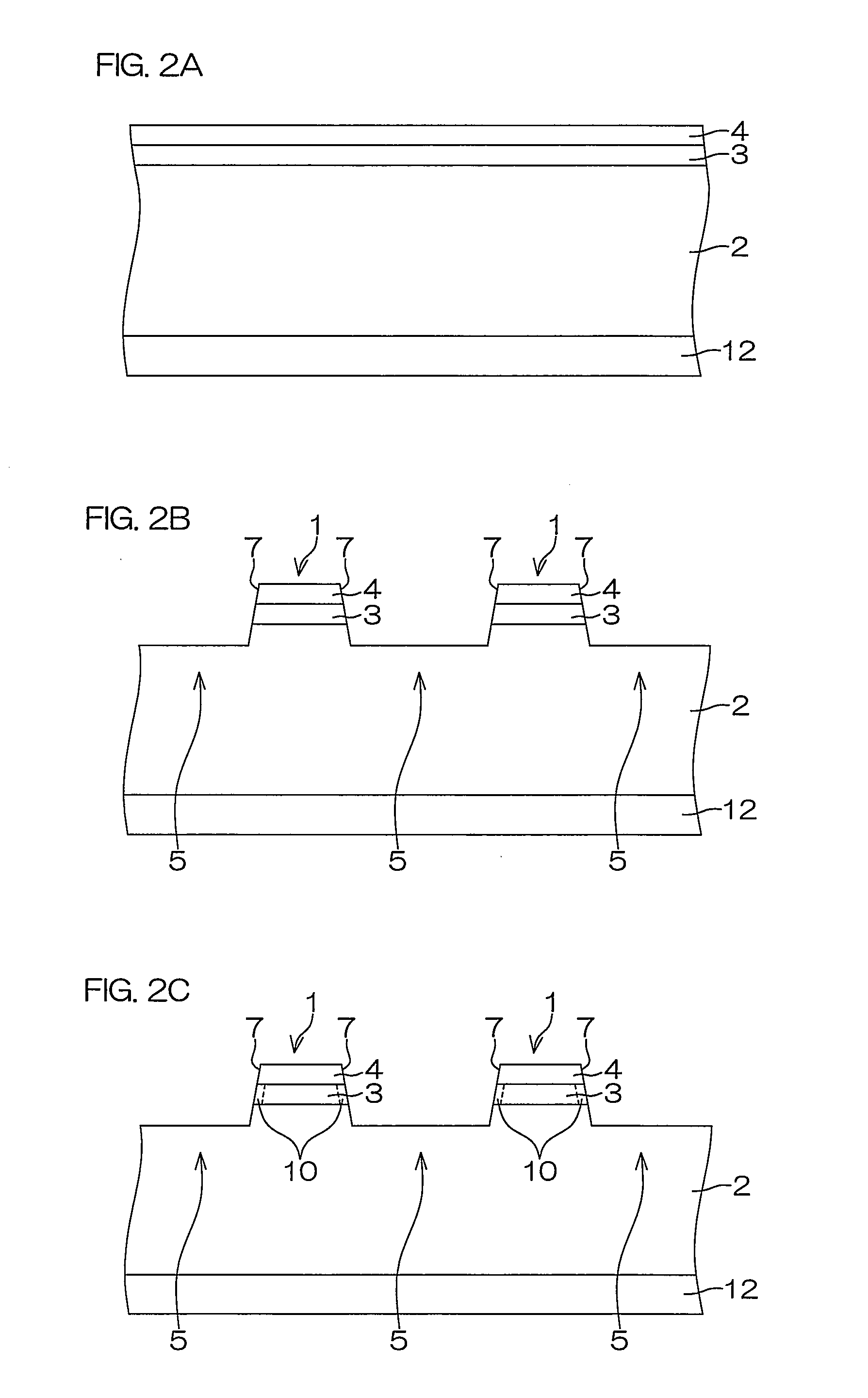
[0103]The susceptor of the treating apparatus having the structure shown in FIG. 3 was made to hold a wafer (a sapphire substrate), and an n-type GaN layer (a first layer) containing Si, a p-type GaN layer (a second layer) containing Mg, an n-type GaN layer (a third layer) containing Si and a p-type GaN layer (a fourth layer) containing Mg were successively grown on the wafer by MOCVD under conditions shown in Table 1 (growth rate: 1.3 μm / h to 1.5 μm / h, thermostat temperature for TMG: about 5° C., thermostat temperature for EtCp2Mg: about 30° C.). TMG and EtCp2Mg were bubbled with H2, and gases generated by the bubbling were fed with the carrier gas (H2). On the other hand, ammonia and silane were fed as pure gases, without employing the carrier gas (H2). Thus, a GaN nitride semiconductor laminated structure consisting of an npnp laminated structure was obtained. The following measurement was performed on the obtained nitride semiconductor laminated structure:

[Table 1]

[0104]Referrin...

example 2

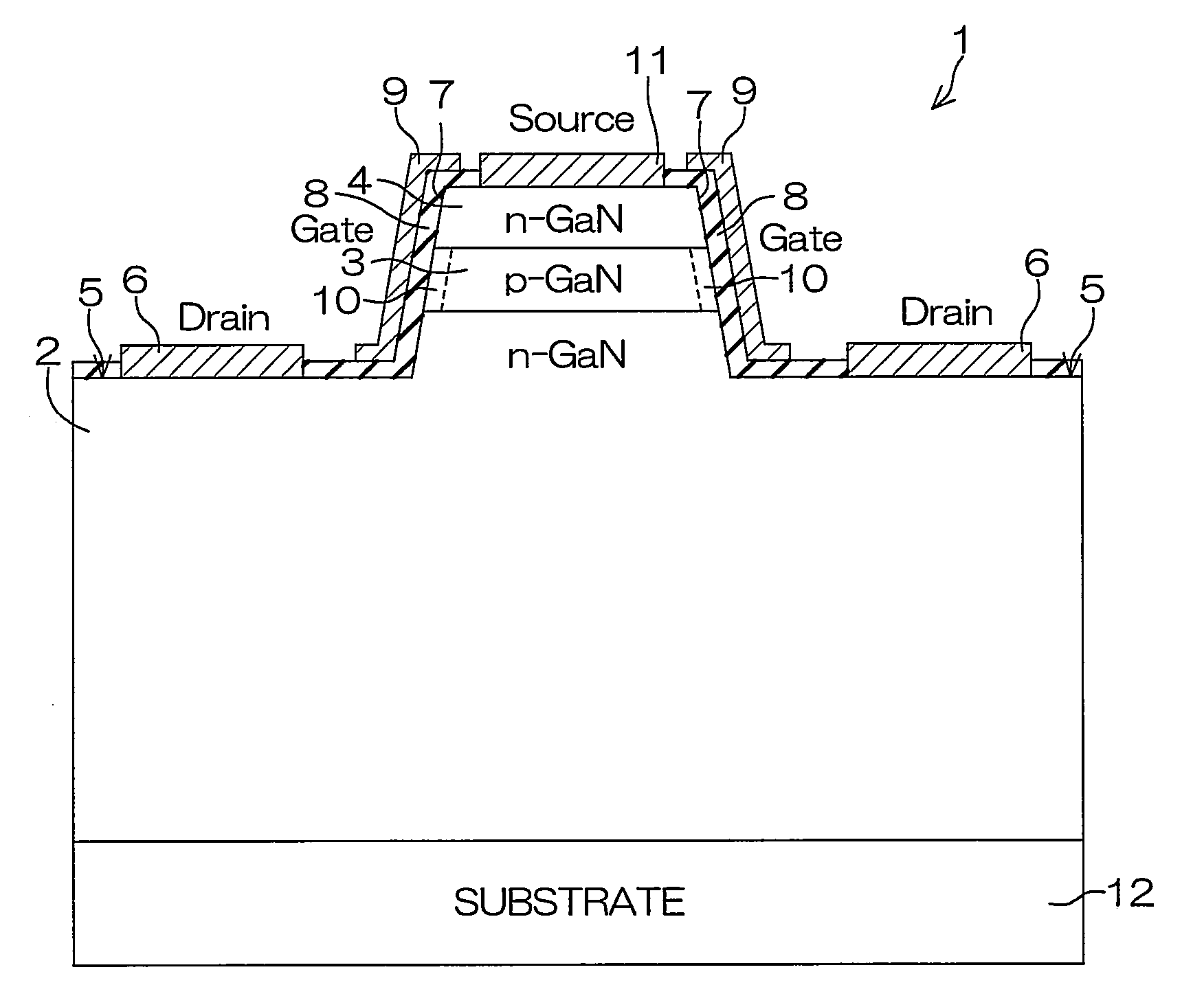
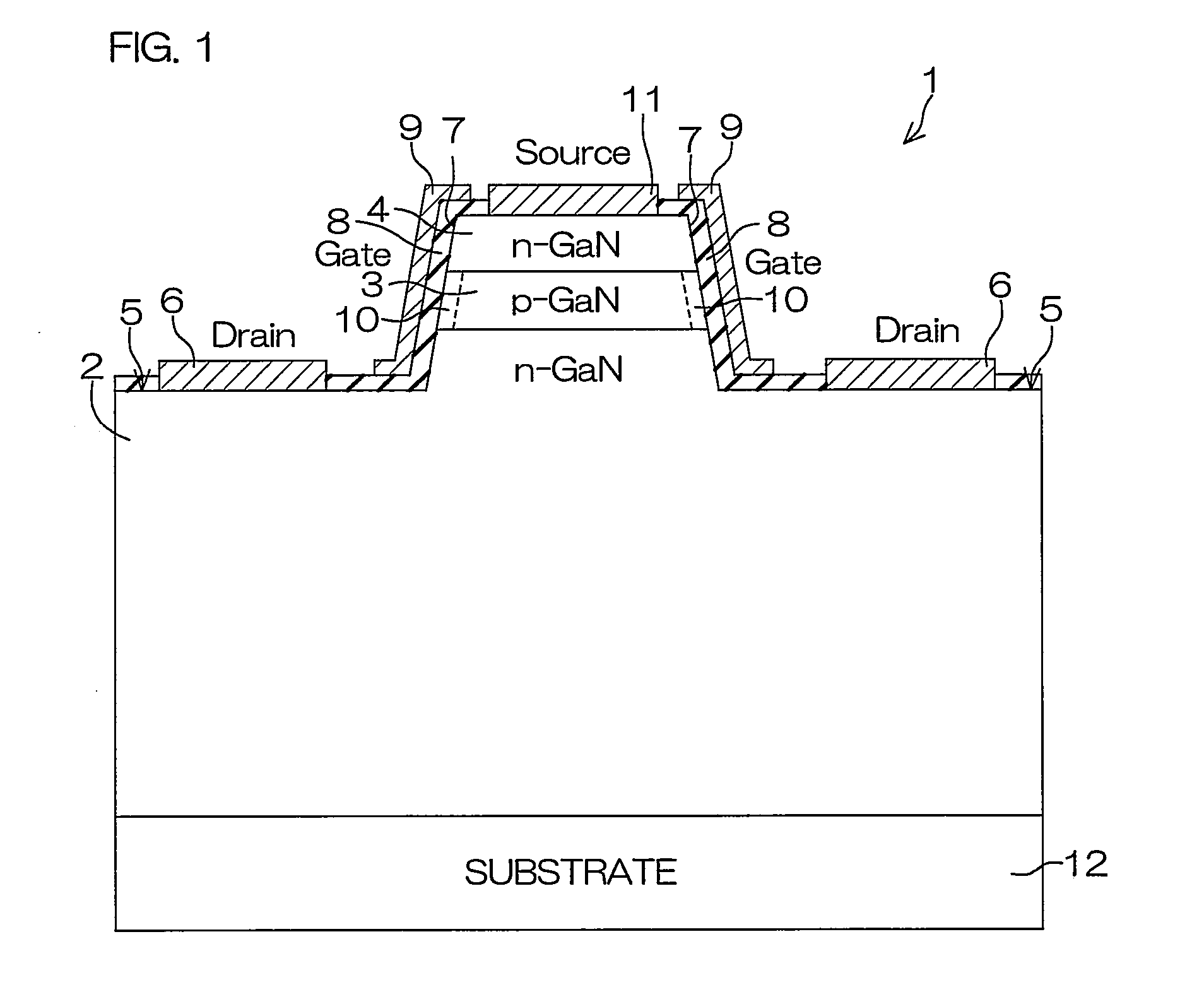
[0110]A field-effect transistor having an npn laminated structure consisting of an n-type GaN layer (a first layer) containing Si, a p-type GaN layer (a second layer) containing Mg and an n-type GaN layer (a third layer) containing Si was prepared on the basis of the manufacturing method illustrated in the aforementioned embodiment.

[0111]Measurement of Gate Voltage-Drain Current Characteristics

[0112]Gate voltage-drain current characteristics of the obtained field-effect transistor were measured. FIGS. 5 and 6 show the results. FIG. 5 shows changes of the drain current (Id) in a case of fixing the gate voltage (Vg) to a constant value and sweeping the drain voltage (Vd). FIG. 6 shows changes of the drain current (Id) in a case of fixing the drain voltage (Vd) to a constant value and sweeping the gate voltage (Vg).

[0113]When the gate voltage (Vg) is 0 V, i.e., when no bias is supplied to a gate electrode, no drain current flows even if a bias is supplied to a drain electrode, as shown...


PUM


Abstract

The method for forming a nitride semiconductor laminated structure according to the present invention includes: a first layer forming step of forming an n-type or i-type first layer composed of a group III nitride semiconductor; a second layer forming step of laminating a p-type second layer composed of a group III nitride semiconductor and containing Mg on the first layer; and a third layer forming step of forming an n-type or i-type third layer composed of a group III nitride semiconductor on the second layer after the second layer forming step.

Description

TECHNICAL FIELD[0001]The present invention relates to a method for forming a nitride semiconductor laminated structure employing group III nitride semiconductors, and a method for manufacturing a nitride semiconductor device employing group III nitride semiconductors.PRIOR ART[0002]In general, a power device employing a silicon semiconductor is employed for a power amplifier circuit, a power supply circuit, a motor driving circuit or the like.[0003]However, improvement in withstand voltage, reduction in resistance and improvement in speed of a silicon device are now reaching limits due to the theoretical limit of the silicon semiconductor, and it is becoming difficult to satisfy requirements of the market.[0004]Therefore, development of a GaN device having characteristics such as a high withstand voltage, a high-temperature operation, a high current density, high-speed switching and small on-resistance is examined (refer to Non-Patent Document 1, for example).[0005]A hitherto propos...

Claims


Application Information

Patent Timeline
IPC IPC(8): H01L21/336H01L21/20H01L21/205H01L29/12H01L29/78H01L29/786
CPCH01L21/0254H01L21/02573H01L29/66462H01L21/86H01L29/2003H01L21/0262
Inventor OTAKE, HIROTAKAOHTA, HIROAKIEGAMI, SHIN
Owner ROHM CO LTD
Learn More