Four terminal multi-junction thin film photovoltaic device and method

Inactive Publication Date: 2010-03-04
STION
View PDF40 Cites 19 Cited by
  • Summary
  • Abstract
  • Description
  • Claims
  • Application Information

AI Technical Summary

Benefits of technology

[0011]Many benefits are achieved by ways of present invention. For example, the present invention uses starting materials that are commercially available to form a thin film of semiconductor bearing material overlying a suitable substrate member. The thin film of semiconductor bearing material can be further processed to form a semiconductor thin film material of desired characteristics, such as atomic stoichiometry, impurity concentration, carrier concentration, doping, and others. In a specific embodiment, the upper cell is configured to selectively filter certain wavelengths, while allowing others to pass and be processed in the lower cell. In a preferred embodiment, the upper cell configuration occurs using a preferred electrode layer, which can be combined or varied. In a preferred embodiment, the present configuration would replace the TCO, which is often an n+ type material, which is formed against a p type absorber leading to limitations, e.g., second junction. In a preferred embo

Problems solved by technology

Unfortunately, the supply of petrochemical fuel is limited and essentially fixed based upon the amount available on the planet Earth.
Additionally, as more people use petroleum products in growing amounts, it is rapidly becoming a scarce resource, which will eventually become depleted over time.
Although solar energy is environmentally clean and has been successful to a point, many limitations remain to be resolved before it becomes widely used throughout the world.
However, crystalline materia

Method used


Image

  • Four terminal multi-junction thin film photovoltaic device and method
  • Four terminal multi-junction thin film photovoltaic device and method
  • Four terminal multi-junction thin film photovoltaic device and method

Examples


Example

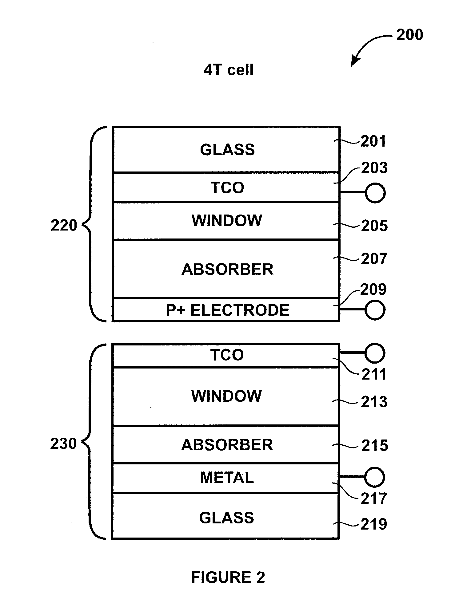
[0016]According to embodiments of the present invention, a method and a structure for forming thin film semiconductor materials for photovoltaic applications are provided. More particularly, the present invention provides a method and structure for manufacture of high efficiency multi-junction thin film photovoltaic cells. Merely by way of example, the present method and materials include absorber materials made of copper indium disulfide species, copper tin sulfide, iron disulfide, or others for multi-junction cells.

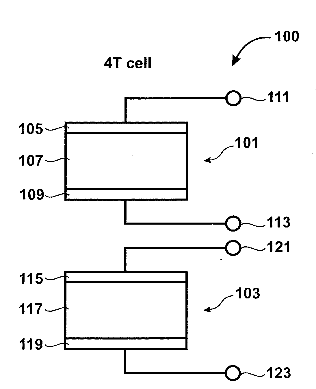
[0017]FIG. 1 is a simplified diagram 100 of a four terminal multi-junction photovoltaic cell according to an embodiment of the present invention. The diagram is merely an illustration and should not unduly limit the scope of the claims herein. One of ordinary skill in the art would recognize other variations, modifications, and alternatives. As shown, the present invention provides a multi-junction photovoltaic cell device 100. The device includes a lower cell 103 and a...


PUM


Abstract

A multi-junction photovoltaic cell device. The device includes a lower cell and an upper cell, which is operably coupled to the lower cell. In a specific embodiment, the lower cell includes a lower glass substrate material, e.g., transparent glass. The lower cell also includes a lower electrode layer made of a reflective material overlying the glass material. The lower cell includes a lower absorber layer overlying the lower electrode layer. In a specific embodiment, the absorber layer is made of a semiconductor material having a band gap energy in a range of Eg=0.7 to 1 eV, but can be others. In a specific embodiment, the lower cell includes a lower window layer overlying the lower absorber layer and a lower transparent conductive oxide layer overlying the lower window layer. The upper cell includes a p+ type transparent conductor layer overlying the lower transparent conductive oxide layer. In a preferred embodiment, the p+ type transparent conductor layer is characterized by traversing electromagnetic radiation in at least a wavelength range from about 700 to about 630 nanometers and filtering electromagnetic radiation in a wavelength range from about 490 to about 450 nanometers. In a specific embodiment, the upper cell has an upper p type absorber layer overlying the p+ type transparent conductor layer. In a preferred embodiment, the p type conductor layer made of a semiconductor material has a band gap energy in a range of Eg=1.6 to 1.9 eV, but can be others. The upper cell also has an upper n type window layer overlying the upper p type absorber layer, an upper transparent conductive oxide layer overlying the upper n type window layer, and an upper glass material overlying the upper transparent conductive oxide layer.

Description

CROSS-REFERENCES TO RELATED APPLICATIONS[0001]This application claims priority to U.S. Provisional Patent Application No. 61 / 092,732, filed Aug. 28, 2008, entitled “FOUR TERMINAL MULTI-JUNCTION THIN FILM PHOTOVOLTAIC DEVICE AND METHOD” by inventor HOWARD W. H. LEE commonly assigned and incorporated by reference herein for all purposes.STATEMENT AS TO RIGHTS TO INVENTIONS MADE UNDER FEDERALLY SPONSORED RESEARCH AND DEVELOPMENT[0002]NOT APPLICABLEREFERENCE TO A “SEQUENCE LISTING,” A TABLE, OR A COMPUTER PROGRAM LISTING APPENDIX SUBMITTED ON A COMPACT DISK[0003]NOT APPLICABLEBACKGROUND OF THE INVENTION[0004]The present invention relates generally to photovoltaic materials and manufacturing method. More particularly, the present invention provides a method and structure for manufacture of high efficiency multi-junction thin film photovoltaic cells. Merely by way of example, the present method and materials include absorber materials made of copper indium disulfide species, copper tin su...

Claims


Application Information

Patent Timeline
IPC IPC(8): H01L31/052
CPCH01L31/022466H01L31/032H01L31/043H01L31/0749Y02E10/541H01L31/0725H01L31/022483Y02P70/50
Inventor LEE, HOWARD W.H.
Owner STION
Why Eureka
Try Eureka