Mulit-layer embedded capacitance and resistance substrate core

a resistance substrate and capacitance core technology, applied in the association of feed-through capacitors, printed circuit non-printed electric components, fixed capacitors, etc., can solve the problems of low parasitic activity, inability of dielectric layers to withstand substantial voltage, and formation of holes, etc., to achieve low parasitic activity and low inductance

Inactive Publication Date: 2010-03-11
TTM TECH NORTH AMERICA LLC
View PDF28 Cites 31 Cited by
  • Summary
  • Abstract
  • Description
  • Claims
  • Application Information

AI Technical Summary

Benefits of technology

[0026]In accordance with the present invention, there is provided a laser drillable, multi-layer embedded capacitance and resistance layers core substrate capable of providing bulk decoupling capacitance and resistance with low inductance and low parasitics. Multiple capacitance layers with variable capacitance density and multiple resistance layers with variable resistivity provide a wide range of capacitor and resistor values. multi-layer embedded capacitance and resistance substrate core. At least one layer of resistance material is provided. The layer of resistance material has a layer of electrically conductive material embedded therein. At least one layer of capacitance material of high dielectric constant is disposed on the layer of resistance material. This core substrate can further be circuitized to make a finished printed wiring board or chip carrier where multiple embedded capacitors with variable capacitance density and multiple embedded resistance layer with variable resistivity replace most of the surface mount capacitors and resistors. Thru-holes are formed by laser.

Problems solved by technology

The discrete passive devices occupy a high percentage of the surface area of the completed substrate, which is undesirable because of the increased demand for miniaturization of products.
Because of such external positioning, however, these components still utilize, albeit less than if in singular form, valuable board real estate.
The distribution within the dielectric layer of particles of different size often presents major obstacles to thru-hole formation where the thru-holes are of extremely small diameter, also referred to in the industry as micro-vias, due to the presence of the larger particles.
Another problem associated with pre-fired ceramic nano-powders is the ability for the dielectric layer to withstand substantial voltage without breakdown occurring across the layer.
This is even further undesirable because, as indicated by the equation cited above, greater planar capacitance may also be achieved by reducing the thickness of the dielectric layer.
That is, the resulting PCB still requires the utilization of external devices thereon, and thus does not afford the PCB external surface area real estate savings mentioned above.
Although the pre-fired and ground dielectric formulations produced by solid phase reactions are acceptable for many electrical applications, these suffer from several disadvantages.
First, the milling step serves as a source of contaminants, which can adversely affect electrical properties.
Second, the milled product consists of irregularly shaped fractured aggregates which are often too large and possess a wide particle size distribution, 500-20,000 nm.
Consequently, films produced using these powders are limited to thicknesses greater than the size of the largest particle.
Third, powder suspensions or composites produced using pre-fired ground ceramic powders must be used immediately after dispersion, due to the high sedimentation rates associated with large particles.
It is thus clear that methods of making PCBs which rely on the advantageous features of using nano-powders as part of the PCB's internal components possess various undesirable aspects which are detrimental to providing a PCB with optimal functioning capabilities when it comes to internal capacitance or other electrical operation.

Method used


Image

  • Mulit-layer embedded capacitance and resistance substrate core
  • Mulit-layer embedded capacitance and resistance substrate core
  • Mulit-layer embedded capacitance and resistance substrate core

Examples


example one

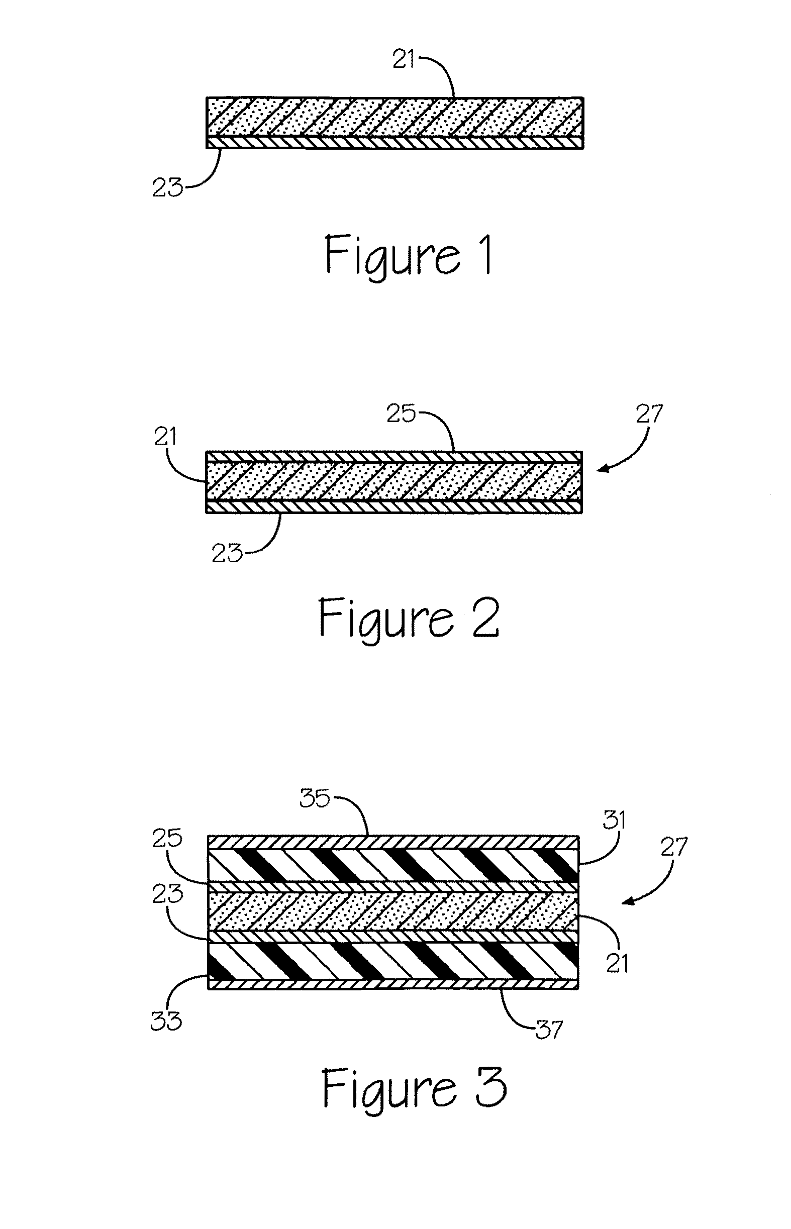
[0071]38.5 grams (gm) of epoxy novolac resin (e.g., one sold under product designation “LZ 8213” by Huntsman) containing about 35 percent by weight methyl ethyl ketone, and catalyzed with about 0.015 parts per hundred (PPH) of 2-methyl-imidazole and 12.8 gm of a high molecular weight, reactive thermoplastic phenoxy resin (e.g., the aforementioned one sold under the product name “PKHS-40” by the InChem Corporation) containing 60 percent by weight methyl ethyl ketone, were mixed together with 100 gm of barium titanate (BaTiO3) powder (available from Cabot Corporation, having a business location in Boyertown, Pa.). The barium titanate powder included a mean particle size of 0.12 microns and a surface area of 8.2 m2 / gm. Also mixed in with this composition was 20 gm of methyl ethyl ketone. The composition was ball milled for one day, after which a thin coating of this well dispersed composition was wire-rod coated on a copper substrate (a copper foil) and dried at about 130 degrees C. fo...

example two

[0072]50 gm of epoxy novolac resin (e.g., the “LZ 8213” above by Huntsman) containing about 35 percent by weight methyl ethyl ketone and catalyzed with about 0.015 PPH of 2-methyl-imidazole, and 19.2 gm of the high molecular weight, reactive thermoplastic phenoxy resin “PKHS-40” (containing 60 percent by weight methyl ethyl ketone), were mixed together with 111 gm of barium titanate (BaTiO3) powder from Cabot Corporation having the same mean particle size and surface area as in Example One (0.12 microns and 8.2 m2 / gm, respectively). Also mixed in with this composition was 20 gm of methyl ethyl ketone. As also in Example One, the composition was ball milled for one day, after which a thin coating of this mixed composition was deposited on a copper substrate (a copper foil) and dried at about 130 degrees C. for three minutes in a standard convection oven. This heating also served to substantially remove all residual organic solvents. Following removal and cooling to room temperature, ...


PUM

PropertyMeasurementUnit
capacitanceaaaaaaaaaa
resistanceaaaaaaaaaa
electrically conductiveaaaaaaaaaa

Abstract

A multi-layer imbedded capacitance and resistance substrate core. At least one layer of resistance material is provided. The layer of resistance material has a layer of electrically conductive material embedded therein. At least one layer of capacitance material of high dielectric constant is disposed on the layer of resistance material. Thru-holes are formed by laser.

Description

RELATED PATENT APPLICATIONS[0001]The present patent application is related to U.S. Published Patent Application No. 2007 / 0010064 upon application filed Feb. 13, 2006 for METHOD OF MAKING A CAPACITIVE SUBSTRATE USING PHOTOIMAGEABLE DIELECTRIC FOR USE AS PART OF A LARGER CIRCUITIZED SUBSTRATE, METHOD OF MAKING SAID CIRCUITIZED SUBSTRATE AND METHOD OF MAKING AN INFORMATION HANDLING SYSTEM INCLUDING SAID CIRCUITIZED SUBSTRATE, and U.S. Published Patent Application No. 2007 / 0177331 upon application filed Apr. 4, 2007 for NON-FLAKING CAPACITOR MATERIAL, CAPACITIVE SUBSTRATE HAVING AN INTERNAL CAPACITOR THEREIN INCLUDING SAID NON-FLAKING CAPACITOR MATERIAL, AND METHOD OF MAKING A CAPACITOR MEMBER FOR USE IN A CAPACITIVE SUBSTRATE.FIELD OF THE INVENTION[0002]The present invention relates to printed circuit board substrates and, more particularly, to a printed circuit board substrate having an embedded capacitance and resistance core.BACKGROUND OF THE INVENTION[0003]Circuitized substrates su...

Claims


Application Information

Patent Timeline
Patent Type & Authority Applications(United States)
IPC IPC(8): H03H7/00H05K3/30
CPCH05K1/023H05K1/0234H05K1/162H05K1/167H05K3/0032H05K3/0038Y10T29/4913H05K3/4652H05K2201/0209H05K2201/0355H05K2203/0361Y10T428/12493Y10T428/24917H05K3/429Y10T428/31511
Inventor DAS, RABINDRA N.LAUFFER, JOHN M.MEMIS, IRVINGROSSER, STEVEN G.
Owner TTM TECH NORTH AMERICA LLC
Why Eureka
Try Eureka