Display device

a technology of display device and display screen, which is applied in the direction of semiconductor devices, instruments, electrical equipment, etc., can solve the problem that the transistor is not always suitable for a larger glass substra

Active Publication Date: 2010-03-18
SEMICON ENERGY LAB CO LTD
View PDF46 Cites 191 Cited by
  • Summary
  • Abstract
  • Description
  • Claims
  • Application Information

AI Technical Summary

Benefits of technology

[0016]According to an embodiment of the present invention, a display device having a structure suitable as a protective circuit can be provided by forming the protective circuit with use of a non-linear element including an oxide semiconductor. When the non-linear element has a stacked structure where the gate insulating layer and the oxide semiconductor layer are in contact with each other, a defect of a protective circuit which is caused by peeling of a thin film can be prevented.

Problems solved by technology

On the other hand, a thin film transistor manufactured using polycrystalline silicon has high field effect mobility, but a crystallization step such as laser annealing is necessary and such a transistor is not always suitable for a larger glass substrate.

Method used


Image

  • Display device
  • Display device
  • Display device

Examples


embodiment 1

[0044]In Embodiment 1, an example of a display device including a pixel portion and a protective circuit including a non-linear element provided around the pixel portion is described with reference to drawings.

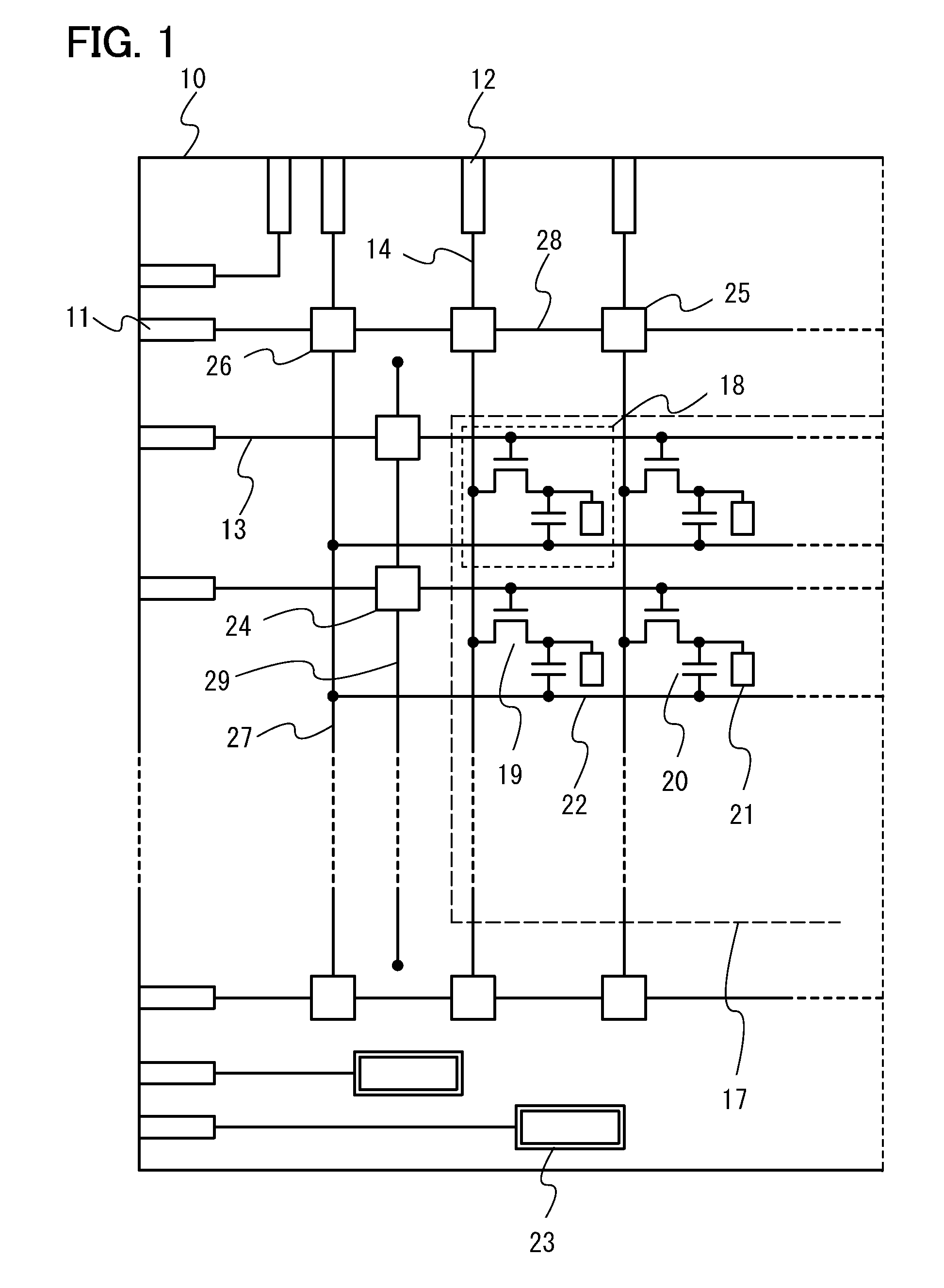
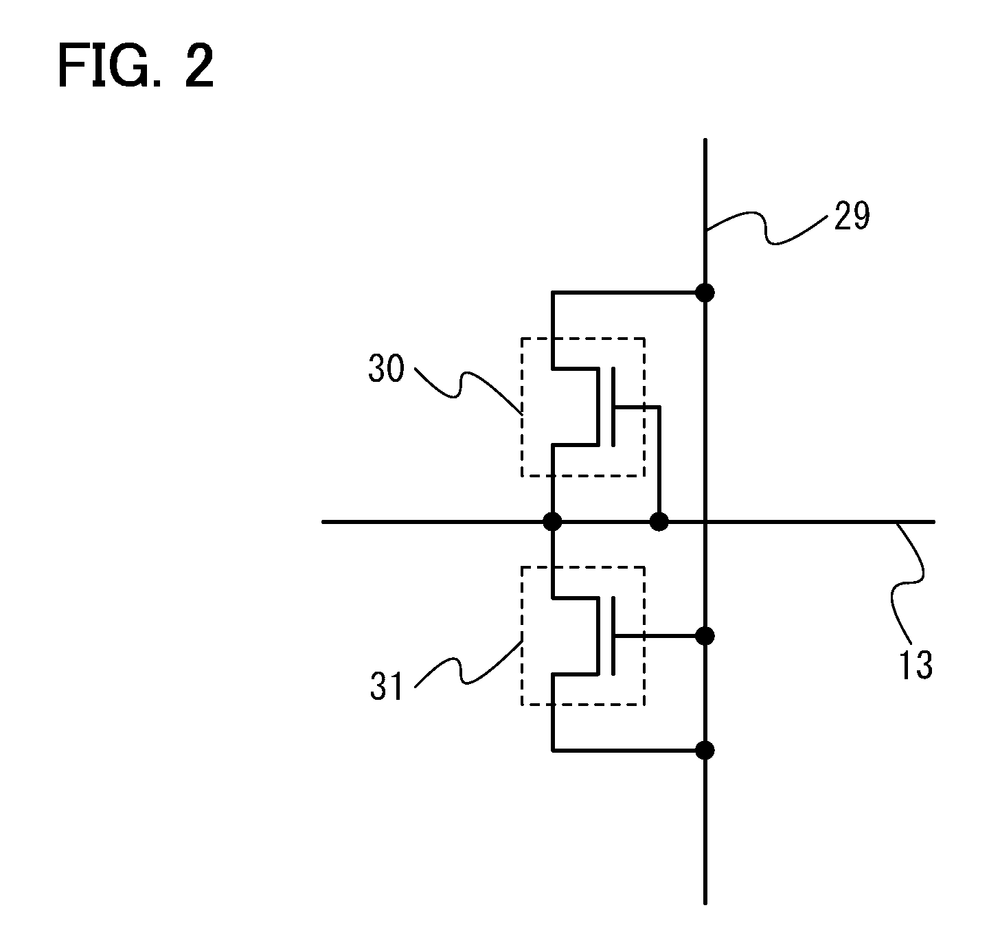
[0045]FIG. 1 illustrates a positional relationship among signal input terminals, scan lines, signal lines, protective circuits including non-linear elements, and a pixel portion in a display device. Over a substrate 10 having an insulating surface, scan lines 13 and signal lines 14 intersect with each other to form a pixel portion 17.

[0046]The pixel portion 17 includes a plurality of pixels 18 arranged in matrix. The pixel 18 includes a pixel transistor 19 connected to the scan line 13 and the signal line 14, a storage capacitor portion 20, and a pixel electrode 21.

[0047]In the pixel structure illustrated here, one electrode of the storage capacitor portion 20 is connected to the pixel transistor 19 and the other electrode is connected to a capacitor line 22. Moreover, the pix...

embodiment 2

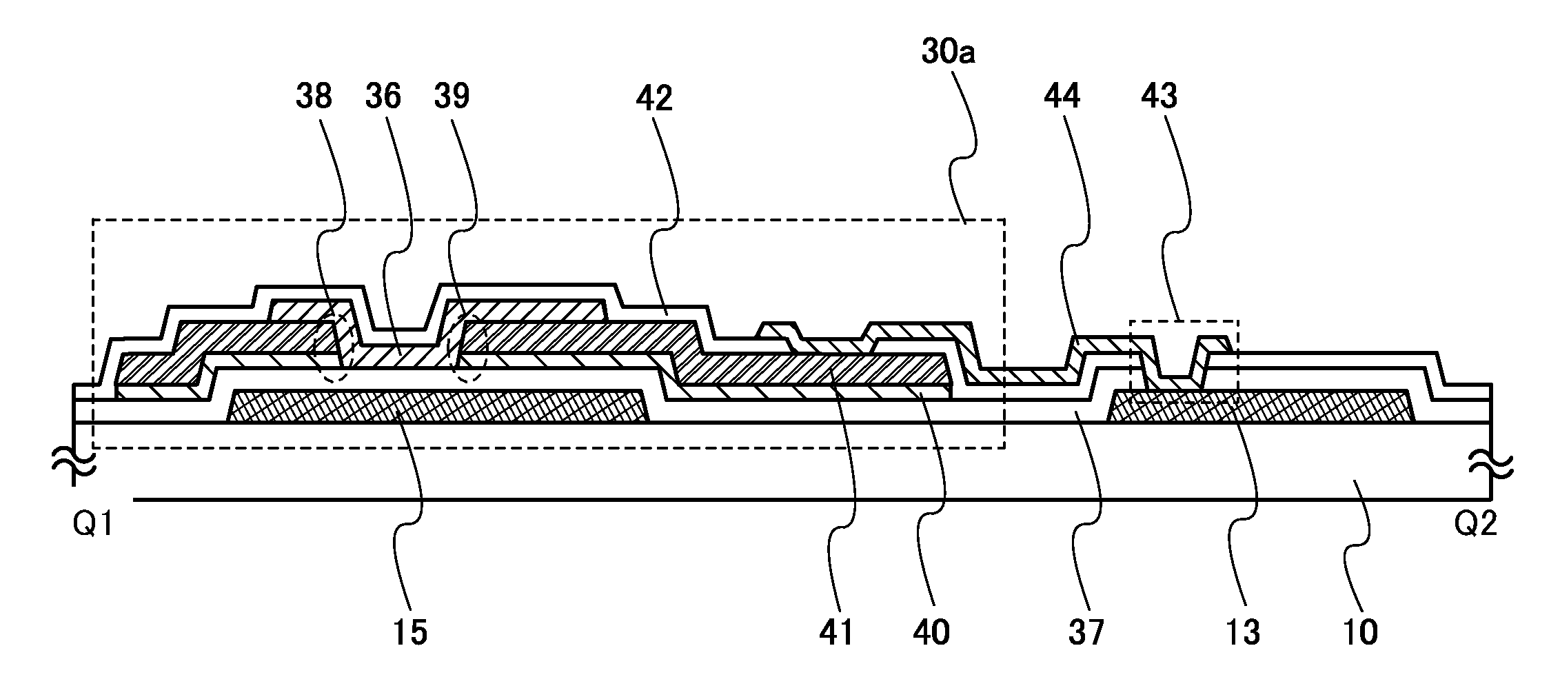
[0069]In Embodiment 2, an embodiment of a process for manufacturing the protective circuit illustrated in FIG. 4A in Embodiment 1 is described with reference to FIGS. 6A to 6C and FIGS. 7A to 7C. FIGS. 6A to 6C and FIGS. 7A to 7C are cross-sectional views taken along line Q1-Q2 of FIG. 4A.

[0070]In FIG. 6A, a glass substrate of barium borosilicate glass, aluminoborosilicate glass, aluminosilicate glass, or the like available in the market can be used as the substrate 100 having a light-transmitting property. For example, a glass substrate which includes more barium oxide (BaO) than boric acid (B2O3) in composition ratio and whose strain point is 730° C. or higher is preferable. This is because the glass substrate is not strained even in the case where the oxide semiconductor layer is thermally processed at high temperatures of about 700° C.

[0071]Next, a conductive layer is formed entirely over the substrate 100. After that, a resist mask is formed by a first photolithography process,...

embodiment 3

[0095]Embodiment 3 illustrates an example of electronic paper in which a protective circuit and a TFT in a pixel portion are provided over one substrate, as a display device to which an embodiment of the present invention is applied.

[0096]FIG. 10 illustrates active matrix type electronic paper as an example of a display device to which an embodiment of the present invention is applied. A thin film transistor 581 used for a display device can be manufactured in a manner similar to the non-linear element described in Embodiment 2. The thin film transistor 581 has high electrical characteristics and includes a gate insulating layer on which plasma treatment has been performed, a source region and a drain region which are formed using an IGZO semiconductor film of oxygen-deficiency type, a source electrode layer and a drain electrode layer which are in contact with the source region and the drain region respectively, and an IGZO semiconductor layer of oxygen-excess type which is in cont...


PUM


Abstract

A protective circuit includes a non-linear element, which includes a gate electrode, a gate insulating layer covering the gate electrode, a pair of first and second wiring layers whose end portions overlap with the gate electrode over the gate insulating layer and in which a second oxide semiconductor layer and a conductive layer are stacked, and a first oxide semiconductor layer which overlaps with at least the gate electrode and which is in contact with the gate insulating layer, side face portions and part of top face portions of the conductive layer and side face portions of the second oxide semiconductor layer in the first wiring layer and the second wiring layer. Over the gate insulating layer, oxide semiconductor layers with different properties are bonded to each other, whereby stable operation can be performed as compared with Schottky junction. Thus, the junction leakage can be decreased and the characteristics of the non-linear element can be improved.

Description

TECHNICAL FIELD[0001]The present invention relates to a display device including an oxide semiconductor.BACKGROUND ART[0002]A thin film transistor formed over a flat plate such as a glass substrate is manufactured using amorphous silicon or polycrystalline silicon, as typically seen in a liquid crystal display device. A thin film transistor manufactured using amorphous silicon has low field effect mobility, but such a transistor can be formed over a glass substrate with a larger area. On the other hand, a thin film transistor manufactured using polycrystalline silicon has high field effect mobility, but a crystallization step such as laser annealing is necessary and such a transistor is not always suitable for a larger glass substrate.[0003]In view of the foregoing, attention has been drawn to a technique by which a thin film transistor is manufactured using an oxide semiconductor, and such a transistor is applied to an electronic device or an optical device. For example, Patent Doc...

Claims


Application Information

Patent Timeline
Patent Type & Authority Applications(United States)
IPC IPC(8): H01L33/00
CPCG02F1/13624G02F1/1368H01L27/1214H01L27/124H01L29/7869H01L29/66742H01L29/78693H01L27/1225
Inventor YAMAZAKI, SHUNPEIAKIMOTO, KENGOKOMORI, SHIGEKIUOCHI, HIDEKIFUTAMURA, TOMOYAKASAHARA, TAKAHIRO
Owner SEMICON ENERGY LAB CO LTD
Why Eureka
Try Eureka