Surface plasmon optical modulator

a surface plasmon and optical modulator technology, applied in non-linear optics, instruments, optics, etc., can solve the problems of destructively interfering with the reflection at the optical element-metal interface, and achieve the effects of reducing the magnitude of surface plasmon back-scattered, improving the modulation depth of the device, and increasing the probability of electron tunneling

Active Publication Date: 2010-04-29
BOISE STATE UNIVERSITY
View PDF9 Cites 10 Cited by
  • Summary
  • Abstract
  • Description
  • Claims
  • Application Information

AI Technical Summary

Benefits of technology

[0027]Accordingly, an aspect of the present invention is a high-speed optical modulator based on Surface Plasmon-Polariton (SPP) at the hetero-junction of a metal-insulator-semiconductor (MIS) tunneling diode and a phase-matching optical element. The intensity modulation in the SPP due to applied bias on a metal-insulator-semiconductor (MIS) tunneling diode is analyzed by the method of coupling modes in time and shows that manipulating the photon-excited electron tunneling leads to a change in surface plasmon resonance. The electron tunneling in the MIS diode reduces the magnitude of surface plasmon back-scattered field, which destructively interferes with the reflection at an optical element-metal interface, such as a prism-gold (Au) interface or a gold lattice-gold (Au) interface.
[0028]In another aspect of the present invention, the thickness of the Au layer is shown to have a strong influence in the modulation depth of the surface plasmon. To increase the electron tunneling probability, one can devise a resonant tunneling structure or phase-matching optical structure to function as a barrier to improve the modulation depth of the device, particularly for longer wavelength applications. As mentioned above, the coupling of optical waves to a MIS tunneling diode can be achieved by means other than a prism, such as utilizing a periodically modified metal film, such as a gold lattice structure.

Problems solved by technology

The electron tunneling in the MIS diode reduces the magnitude of surface plasmon back-scattered field, which destructively interferes with the reflection at an optical element-metal interface, such as a prism-gold (Au) interface or a gold lattice-gold (Au) interface.

Method used


Image

  • Surface plasmon optical modulator
  • Surface plasmon optical modulator
  • Surface plasmon optical modulator

Examples


worked example

[0048]The following description section is presented to enable one to make and use the invention.

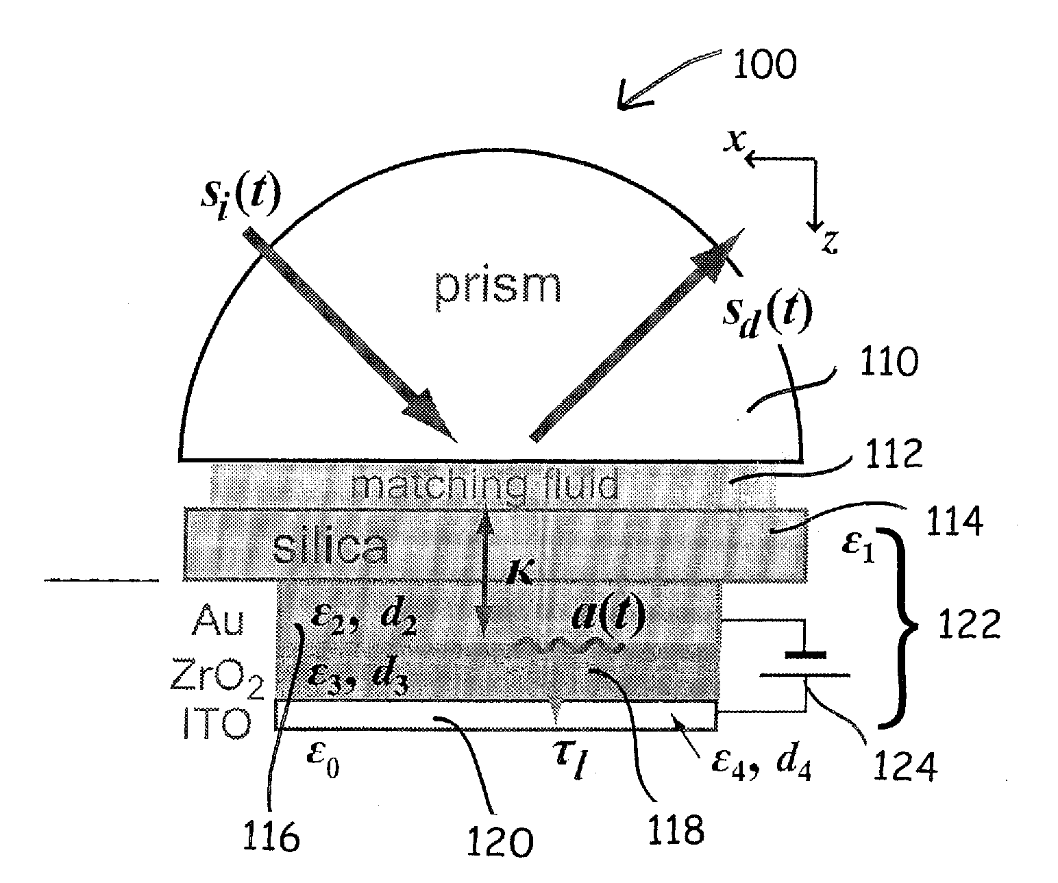
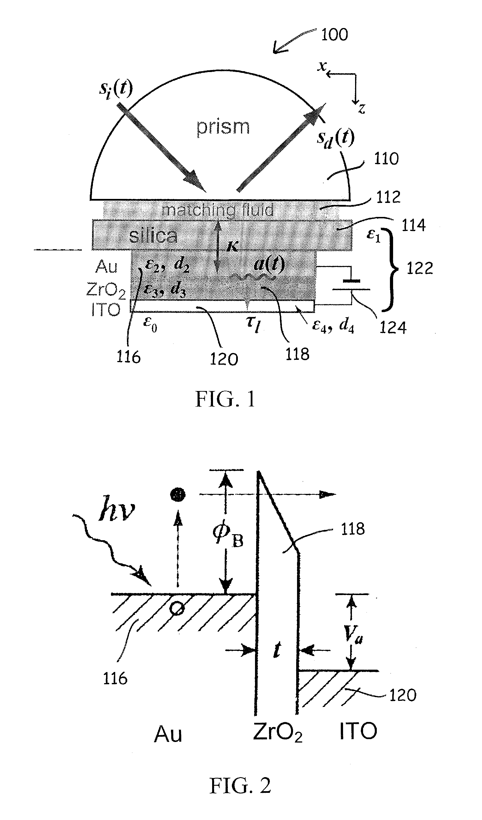
[0049]Referring to FIG. 1, the surface plasmon optical modulator starts from a silica wafer 114 cleaned by common RCA procedure. Overlying a major surface of the substrate is a hetero-structure including subsequent deposition of Au, ZrO2, and ITO by one of many known techniques to form a metal-insulator-semiconductor tunneling diode. It should be understood that tunneling diode could comprise a sandwich of many appropriate insulators wherein it can be used to affect the barrier characteristics described in the patent description. Electrical contacts, from a low loss metal such as Al, Cu, Au, or W, is formed over layer 116 and layer 120. Means such as a battery 124 and switch are connected between layer 116 and 120 for selectively establishing an electric field normal to the planes of layers 116, 118, 120 in MIS diode 122.

[0050]The device 122 is mounted to a semi-cylindrical prism 110 wit...


PUM

PropertyMeasurementUnit
voltageaaaaaaaaaa
voltageaaaaaaaaaa
thicknessaaaaaaaaaa

Abstract

A high-speed optical modulator based on Surface Plasmon-Polariton (SPP) at the hetero-junction of a metal-insulator-semiconductor (MIS) tunneling diode and including a phase-matching optical element, such as a prism or gold-lattice structure, is described. An investigation using the coupled mode theory shows that the applied bias across the hetero-junction changes the optical reflectance of an optically coupled MIS tunneling diode, such as a prism-coupled MIS tunneling diode or a gold lattice-coupled MIS tunneling diode, while the modulation efficiency achievable of the device depends on the thickness of the metal film used to construct the tunneling diode.

Description

[0001]This application claims priority of U.S. provisional patent application Ser. No. 61 / 109,066, filed on Oct. 28, 2008, entitled “Surface plasmon optical modulator,” which is incorporated herein by reference.BACKGROUND OF THE INVENTION[0002]1. Field of the Invention[0003]The present invention relates to optical intensity modulation and in particular to the use of Surface Plasmon-Polaritons (SPPs) in an optical modulator system.[0004]Optical intensity modulators are an important element for integrated optoelectronics. Surface Plasmon-Polaritons (SPPs) are attractive candidates for this use due to their potential to produce high-speed compact devices. SPPs are surface electromagnetic waves that are trapped at the metal-dielectric interface due to their interaction with valence electrons of the conductor. Recent demonstrations of light guiding on closely spaced metal nano-particles have created interest for nano-photonic devices that will merge photonic and electronic functionalitie...

Claims


Application Information

Patent Timeline
Patent Type & Authority Applications(United States)
IPC IPC(8): G02F1/19G02F1/015
CPCG02F1/015G02F2203/10G02F2203/02
Inventor KUANG, WAN
Owner BOISE STATE UNIVERSITY
Why Eureka
Try Eureka