Microwave/millimeter wave sensor apparatus

a sensor apparatus and micro-millimeter wave technology, applied in the direction of instruments, oscillation generators, antennas, etc., can solve the problems of circuit performance degradation, circuit integration limit, connecting portions of functional circuits, etc., and achieve simple structure, simple structure, and high detection sensitivity.

Active Publication Date: 2010-05-13
NAT INST OF INFORMATION & COMM TECH
View PDF47 Cites 32 Cited by
  • Summary
  • Abstract
  • Description
  • Claims
  • Application Information

AI Technical Summary

Benefits of technology

[0040]According to the fourteenth aspect of the present invention, the harmonic selecting unit is placed at an appropriate distance from the radiation face side of the radiation type oscillator, and serves as a frequency selective circuit pattern face that selectively filters radio waves of predetermined frequency. Thus, a harmonic selecting unit can be formed with a simple structure.
[0041]According to the fifteenth aspect of the present invention, a beam radiation type resonator formed with two partially transmissive reflecting faces facing each other is placed at an appropriate distance from the radiation face side of the radiation type oscillator, and the harmonic selecting unit adjusts the resonance frequency of the beam radiation type resonator to desired harmonic frequency. Thus, a harmonic selecting unit can be formed with a simple structure.
[0042]According to the sixteenth aspect of the present invention, the harmonic selecting unit is a waveguide filter that selectively passes and emits desired harmonic. With this arrangement, the radiation beam can be sharpened while a certain opening is maintained at the waveguide outlet, and higher detection sensitivity can be achieved.

Problems solved by technology

In such a microwave / millimeter wave sensor apparatus formed by connecting individual functional circuits, there is a limit to high-density integration of circuits.
Particularly, in millimeter wave bands, the loss due to the connecting portions between the functional circuits and the loss due to the transmission line become main causes of circuit performance degradation.

Method used


Image

  • Microwave/millimeter wave sensor apparatus
  • Microwave/millimeter wave sensor apparatus
  • Microwave/millimeter wave sensor apparatus

Examples


tenth embodiment

[0127]FIG. 13 is a circuit structure diagram of a microwave / millimeter wave sensor apparatus according to a tenth embodiment. Direct current is supplied only from the direct current source DC2 to a radiation type oscillator substrate S10, and a signal analysis processing unit P analyzes and processes sensing signals (IF signals) acquired from the radiation type oscillator substrate S10. In the microwave / millimeter wave sensor apparatus of this embodiment, a voltage-dividing self-bias circuit structure of a drain load bypass type is employed. This circuit structure is the same as the voltage-dividing (series-feedback) self-bias circuit structure employed in the eighth embodiment, except that a capacitor 7c is connected in parallel to the resistor 7 as the IF-band loading unit. The same components as those of the microwave / millimeter wave sensor apparatus of the foregoing embodiments are denoted by the same reference numerals as those used in the foregoing embodiments, and explanation...

eleventh embodiment

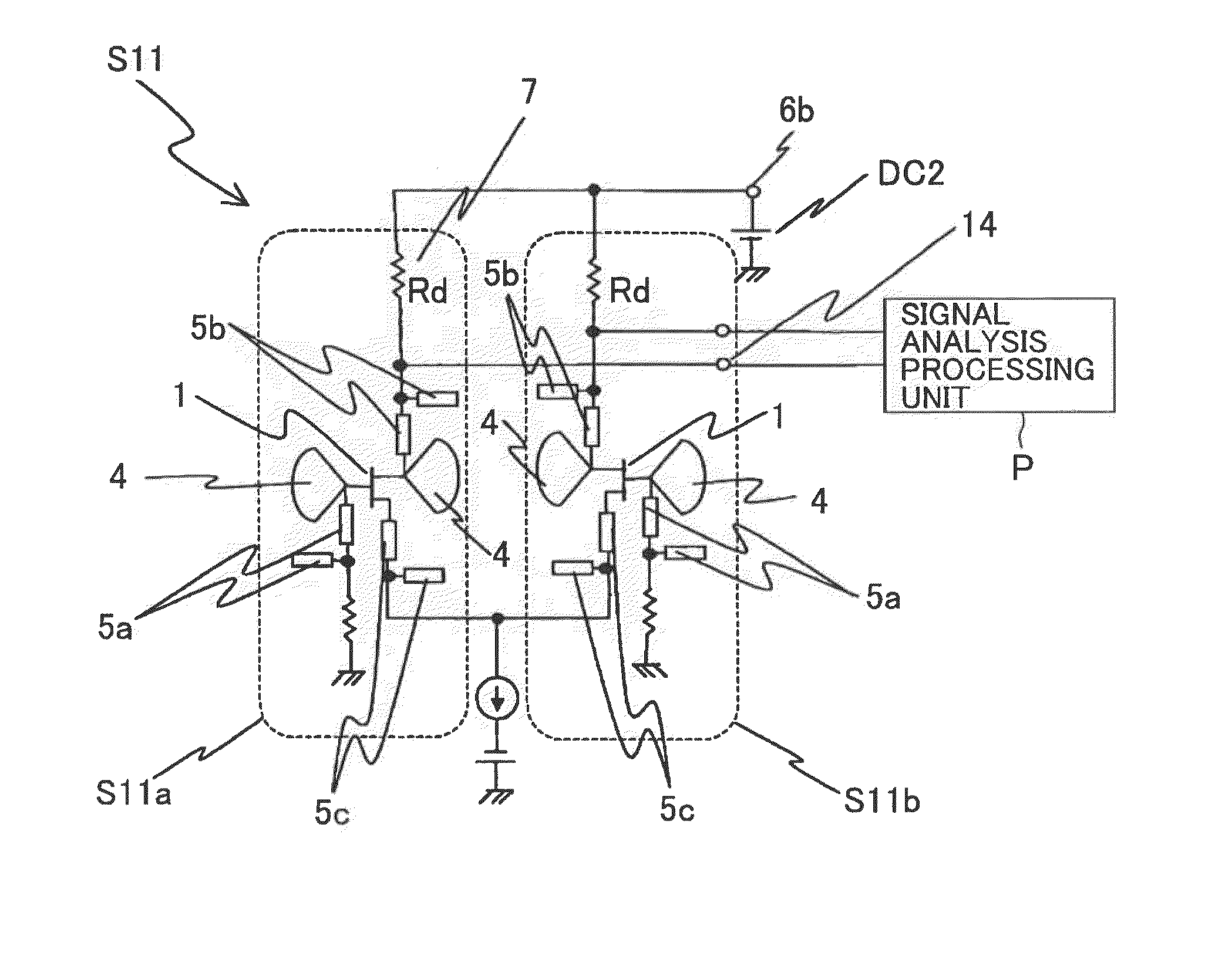
[0129]FIG. 14 is a circuit structure diagram of a microwave / millimeter wave sensor apparatus according to an eleventh embodiment. A radiation type oscillator substrate S11 includes a first radiation type oscillator S11a and a second radiation type oscillator S11b that have the same structures as each other. The sources of the high-frequency transistors 1 of the first and second radiation type oscillators S11a and S11b are connected to each other. With this arrangement, biasing is performed so that the sum of the source currents of the two high-frequency transistors 1 becomes constant, and a differential amplifying operation is performed in the IF band. The same components as those of the microwave / millimeter wave sensor apparatus of the foregoing embodiments are denoted by the same reference numerals as those used in the foregoing embodiments, and explanation of them is not repeated here.

[0130]In the radiation type oscillator substrate S11, the temperature drift that is particularly...

twelfth embodiment

[0131]FIG. 15 is a circuit structure diagram of a microwave / millimeter wave sensor apparatus according to a twelfth embodiment. In a radiation type oscillator substrate S12, an RF choke circuit is not connected to but only a conductor patch 4 is connected to the gate of the high-frequency transistor 1, and a gate-side bias circuit is eliminated by the self-bias of the high-frequency transistor 1 that is oscillating. The same components as those of the microwave / millimeter wave sensor apparatus of the foregoing embodiments are denoted by the same reference numerals as those used in the foregoing embodiments, and explanation of them is not repeated here.


PUM


Abstract

A microwave/millimeter wave sensor apparatus including a planar radiation type oscillator substrate having an inner-layer GND interposed between a front surface side dielectric substrate and a rear surface side dielectric substrate and a pair of conductor patches in an axis-symmetric manner on the side of the front surface layer. A gate and drain of a microwave transistor are respectively connected to the conductor patches to supply power to the gate and the drain of the microwave transistor through a gate-side RF choke circuit and a drain-side RF choke circuit. An impedance line satisfying an oscillation condition is connected to a source and a transmit RF signal in an RF zone as a planar radiation type oscillator is transmitted and a receive RF signal as reflected waves is received from a measured object, thus obtaining an IF signal as the sensing information through homodyne mixing.

Description

TECHNICAL FIELD OF THE INVENTION[0001]The present invention relates to a microwave / millimeter wave sensor apparatus that emits a microwave / millimeter wave band signal onto a measured object, and receives reflected waves from the measured object, thereby detecting the information about the measured object (or performing operation detection, velocity detection, existence detection, and location detection, for example).BACKGROUND OF THE INVENTION[0002]A conventional microwave / millimeter wave sensor apparatus is formed by connecting individual functional circuits, such as a transistor oscillating circuit or a GUNN diode oscillating circuit, a diode mixer circuit, an antenna, a coupler, a divider, and a transmission-reception separating circulator, with the use of a transmission line such as a microstrip line. Such a conventional microwave / millimeter wave sensor apparatus normally uses an oscillation signal of the oscillating circuit as a transmit RF signal, and withdraws part of the osc...

Claims


Application Information

Patent Timeline
Patent Type & Authority Applications(United States)
IPC IPC(8): G01S13/00G01S13/931
CPCG01S7/03G01S7/032G01S13/34G01S13/87G01S13/931G01S2013/9385H01Q9/285H01Q23/00H03B5/1852G01S2013/9375G01S2013/9378H01Q1/2208G01S2013/93274G01S2013/93272G01S2013/93271
Inventor UTAGAWA, HITOSHIMATSUI
Owner NAT INST OF INFORMATION & COMM TECH
Why Eureka
Try Eureka