Thin film transistor and display device

a thin film transistor and display device technology, applied in the direction of semiconductor devices, radio control devices, electrical apparatus, etc., can solve the problems of deterioration in reliability, oxygen desorbed, current-voltage characteristic of thin film transistors, etc., to suppress the deterioration of electric characteristics, improve reliability, and suppress the generation of carriers due to oxygen loss

Active Publication Date: 2010-05-20
JOLED INC
View PDF4 Cites 29 Cited by
  • Summary
  • Abstract
  • Description
  • Claims
  • Application Information

AI Technical Summary

Benefits of technology

[0044]In the thin film transistor 1 of the embodiment, when a voltage (gate voltage Vg) equal to or higher than the predetermined threshold voltage is applied to the gate electrode 12 via a not-shown wiring layer, the channel 14A is formed in the oxide semiconductor film 14, current (drain current Id) flows between the source electrode 16A and the drain electrode 16B, and the thin film transistor 1 functions as a transistor.
[0045]In the embodiment, on the oxide semiconductor film 14 in which the channel 14A is formed, the source electrode 16A and the drain electrode 16B are formed. Each of the source electrode 16A and the drain electrode 16B is obtained by stacking the first, second, and third metal layers 161, 162, and 163 from the side of the oxide semiconductor film 14, and the first metal layer 161 is made of a metal having ionization energy equal to or higher than that of molybdenum. That is, the first metal layer 161 in contact with the oxide semiconductor film 14 is made of a metal which is not susceptible to oxidation.
[0046]On the contrary, in the case where the metal layer in contact with the oxide semiconductor film 14 is made of a metal having ionization energy smaller than that of molybdenum, that is, susceptible to oxidation, oxygen in the oxide semiconductor film 14 is taken to the side of the metal layer with oxidation of the metal layer. Consequently, the oxygen is desorbed to the outside of the oxide semiconductor film 14. Due to loss of oxygen, carriers are generated in the oxide semiconductor layer 14.
[0047]Therefore...

Problems solved by technology

In such an oxide semiconductor, however, oxygen is desorbed with time in manufacture, operation, and the like and, due to this, a current-voltage characteristic of a thin film transistor deteriorates....

Method used


Image

  • Thin film transistor and display device
  • Thin film transistor and display device
  • Thin film transistor and display device

Examples


example

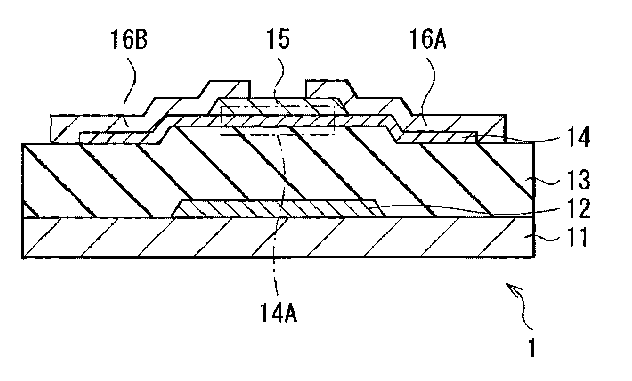
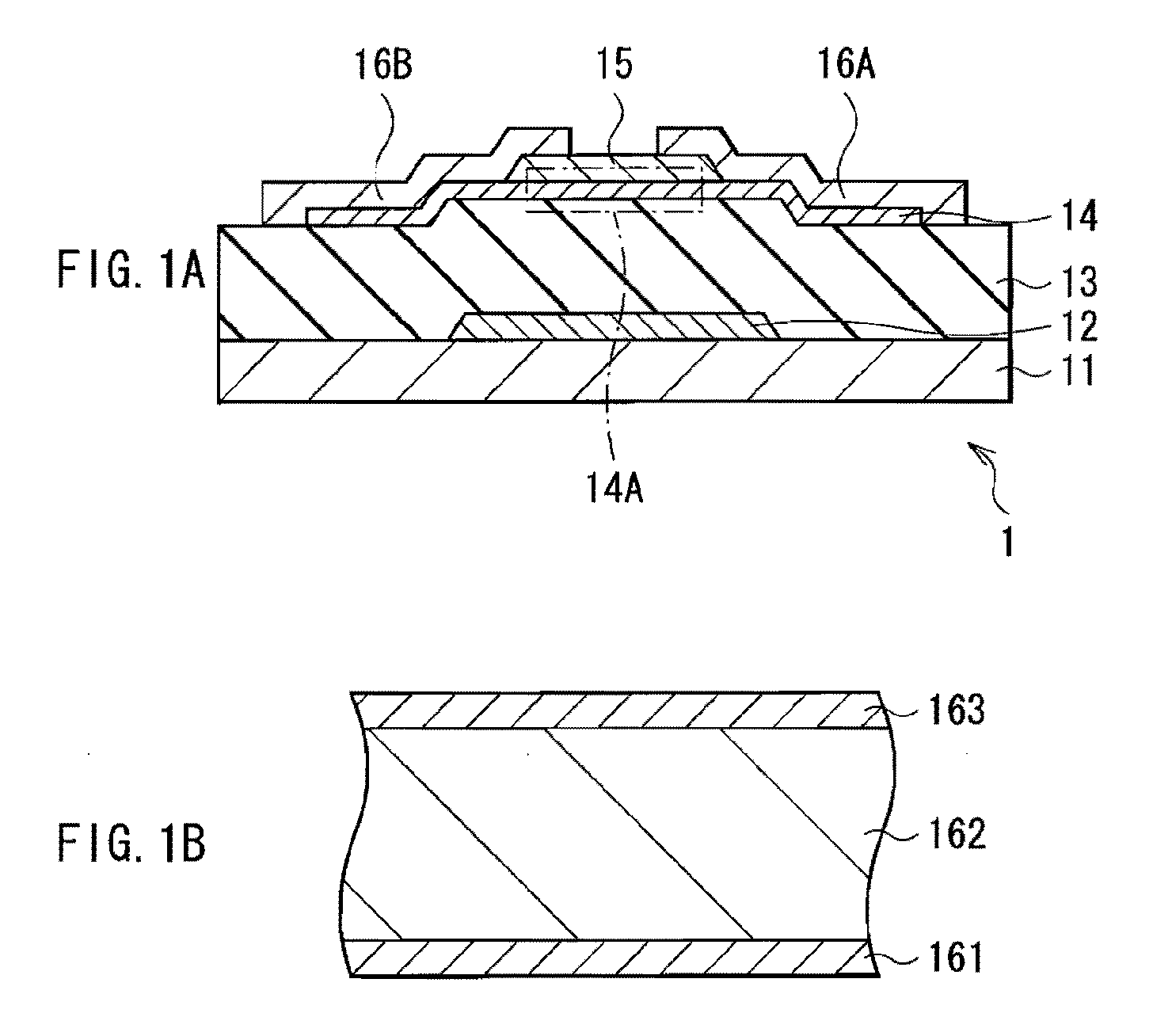
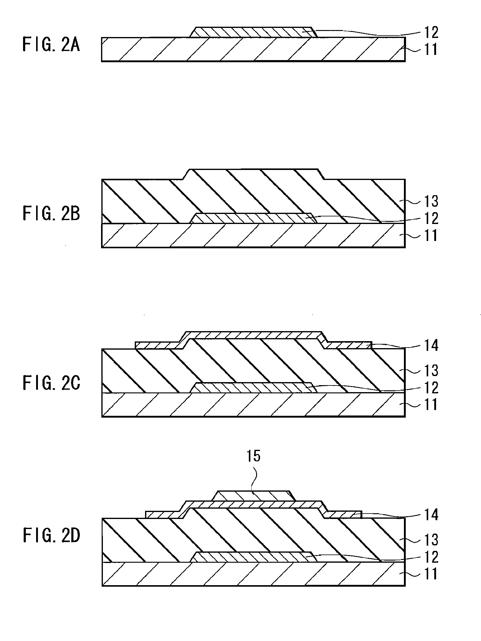
[0053]As an example of the foregoing embodiment, the thin film transistor 1 using molybdenum (50 nm thick) for the first metal layer 161, aluminum (500 nm thick) for the second metal layer 162, and titanium (50 nm thick) for the third metal layer 163 was produced. Molybdenum was used for the gate electrode 12, silicon oxide (SiO) with film thickness 200 nm was used for the gate insulating film 13, In—Ga—Zn—O was used for the oxide semiconductor film 14, and silicon oxide (SiO) with film thickness 200 nm was used for the channel protection film 15. As conditions of annealing process performed after formation of the source electrode 16A and the drain electrode 16B, oxygen concentration in an atmosphere including oxygen (O2) and nitrogen (N2) was set to about 40%, heat treatment temperature was set to 300° C., and treatment time was set to two hours.

[0054]To examine changes in the electric characteristics with time of such a thin film transistor 1, changes in drain current Id (A) with ...


PUM


Abstract

The present invention provides a thin film transistor realizing improved reliability by suppressing deterioration in electric characteristics. The thin film transistor includes an oxide semiconductor film forming a channel; a gate electrode disposed on one side of the oxide semiconductor film via a gate insulating film; and a pair of electrodes formed as a source electrode and a drain electrode in contact with the oxide semiconductor film and obtained by stacking at least first and second metal layers in order from the side of the oxide semiconductor film The first metal layer is made of a metal having ionization energy equal to or higher than molybdenum (Mo), a metal having oxygen barrier property, or a nitride or a silicon nitride of the metal having oxygen barrier property.

Description

BACKGROUND OF THE INVENTION[0001]1. Field of the Invention[0002]The present invention relates to a thin film transistor using an oxide semiconductor film and a display device using the same.[0003]2. Description of the Related Art[0004]In recent years, attention is being paid to a thin film transistor (TFT) using a semiconductor whose main component is an oxide (hereinbelow, called oxide semiconductor) for an active layer. It is known that the electron mobility of the oxide semiconductor is higher than that of amorphous silicon (α-Si) generally used for a liquid crystal display or the like, and the oxide semiconductor has excellent electric characteristics. As such oxide semiconductors, an oxide semiconductor whose main component is zinc oxide (ZnO) (refer to Patent document 1: Japanese Unexamined Patent Application Publication No. 2002-76356), an oxide semiconductor whose main component is In—M—Zn—O (M denotes at least one of gallium (Ga), aluminum (Al), and iron (Fe) (refer to Pate...

Claims


Application Information

Patent Timeline
IPC IPC(8): H01L29/786H01L33/00
CPCH01L29/41733H01L29/7869H01L29/45
Inventor TOKUNAGA, KAZUHIKO
Owner JOLED INC
Why Eureka
Try Eureka