Solid-state imaging device, method for manufacturing solid-state imaging device, and imaging apparatus

a solid-state imaging and imaging device technology, applied in the direction of color television, television system, radio control device, etc., can solve the problems of difficult compatibility between noise reduction and finer pixels, 1/f noise of pixel transistors, etc., to reduce the effective channel width reduce the effect of pixel size and reduced 1/f noise of the transistor in the pixel transistor portion

Active Publication Date: 2010-05-27
SONY CORP
View PDF5 Cites 16 Cited by
  • Summary
  • Abstract
  • Description
  • Claims
  • Application Information

AI Technical Summary

Benefits of technology

[0014]In the solid-state imaging device according to an embodiment of the present invention, the element isolation region disposed in the pixel portion includes the insulating film having a negative charge. Therefore, a hole accumulation layer resulting from the negative charge in the insulating film having the negative charge is generated in the semiconductor substrate immediately under the element isolation region. Noise generation from defects of the interface between the element isolation region and the semiconductor substrate is suppressed by the hole accumulation layer. Furthermore, since the hole accumulation layer is formed by the negative charge, a P-type impurity region formed in the semiconductor substrate immediately under the element isolation region in the related art may be omitted. Alternatively, in the case where a P-type impurity region is formed, the concentration thereof is reduced. Consequently, reduction of the effective channel width of the transistor in the pixel transistor portion due to diffusion of the P-type impurity of the P-type impurity region is suppressed and, thereby, a sufficient effective channel width may be ensured. Therefore, the 1 / f noise of the transistor in the pixel transistor portion is reduced. Put another way, diffusion of the P-type impurity due to the P-type impurity region is suppressed and the pixel size may be reduced correspondingly, while the effective channel width is ensured, and the 1 / f noise is reduced.
[0019]In each of the methods for manufacturing a solid-state imaging device, according to an embodiment of the present invention, the insulating film having a negative charge is formed in the element isolation region disposed in the pixel portion. Therefore, a hole accumulation layer resulting from the negative charge in the insulating film having the negative charge is generated in the semiconductor substrate immediately under the element isolation region. Noise generation from defects of the interface between the element isolation region and the semiconductor substrate is suppressed by the hole accumulation layer. Furthermore, since the hole accumulation layer is formed by the negative charge, a P-type impurity region formed in the semiconductor substrate immediately under the element isolation region in the related art may be omitted. Alternatively, in the case where a P-type impurity region is formed, the concentration thereof is reduced. Consequently, reduction of the effective channel width of the transistor in the pixel transistor portion due to diffusion of the P-type impurity of the P-type impurity region is suppressed and, thereby, a sufficient effective channel width may be ensured. Therefore, the 1 / f noise of the transistor in the pixel transistor portion is reduced. Put another way, diffusion of the P-type impurity due to the P-type impurity region is suppressed and the pixel size may be reduced correspondingly, while the effective channel width is ensured, and the 1 / f noise is reduced.
[0021]In the imaging apparatus according to an embodiment of the present invention, the solid-state imaging device according to an embodiment of the present invention is used. Consequently, reduction of the effective channel width of the transistor in the pixel transistor portion of the solid-state imaging device is suppressed and, thereby, the 1 / f noise of the transistor in the pixel transistor portion is reduced.
[0022]Regarding the solid-state imaging device according to an embodiment of the present invention, diffusion of the P-type impurity due to the P-type impurity region is suppressed and the pixel size may be reduced correspondingly, while the effective channel width is ensured, and the 1 / f noise is reduced. Consequently, noise suppression and a finer pixel are mutually compatible. Therefore, there is an advantage that the image quality of imaging is improved.
[0023]Regarding each of the methods for manufacturing a solid-state imaging device, according to an embodiment of the present invention, diffusion of the P-type impurity due to the P-type impurity region is suppressed and the pixel size may be reduced correspondingly, while the effective channel width is ensured, and the 1 / f noise is reduced. Consequently, noise suppression and a finer pixel are mutually compatible. Therefore, there is an advantage that the image quality of imaging is improved.
[0024]Regarding the imaging apparatus according to an embodiment of the present invention, since the solid-state imaging device, in which noise reduction and a finer pixel are mutually compatible, according to an embodiment of the present invention is used, there is an advantage that the image quality of imaging is improved because of higher image quality and higher sensitivity.

Problems solved by technology

The present inventor has recognized that it is difficult to increase a channel width because a pixel has been made finer and if an effective channel width is reduced, the 1 / f noise of a pixel transistor portion, in particular an amplifying transistor, deteriorates and, therefore, the compatibility between noise reduction and a finer pixel is difficult.

Method used


Image

  • Solid-state imaging device, method for manufacturing solid-state imaging device, and imaging apparatus
  • Solid-state imaging device, method for manufacturing solid-state imaging device, and imaging apparatus
  • Solid-state imaging device, method for manufacturing solid-state imaging device, and imaging apparatus

Examples


first embodiment

[0040]One Example of Configuration of Solid-State Imaging Device

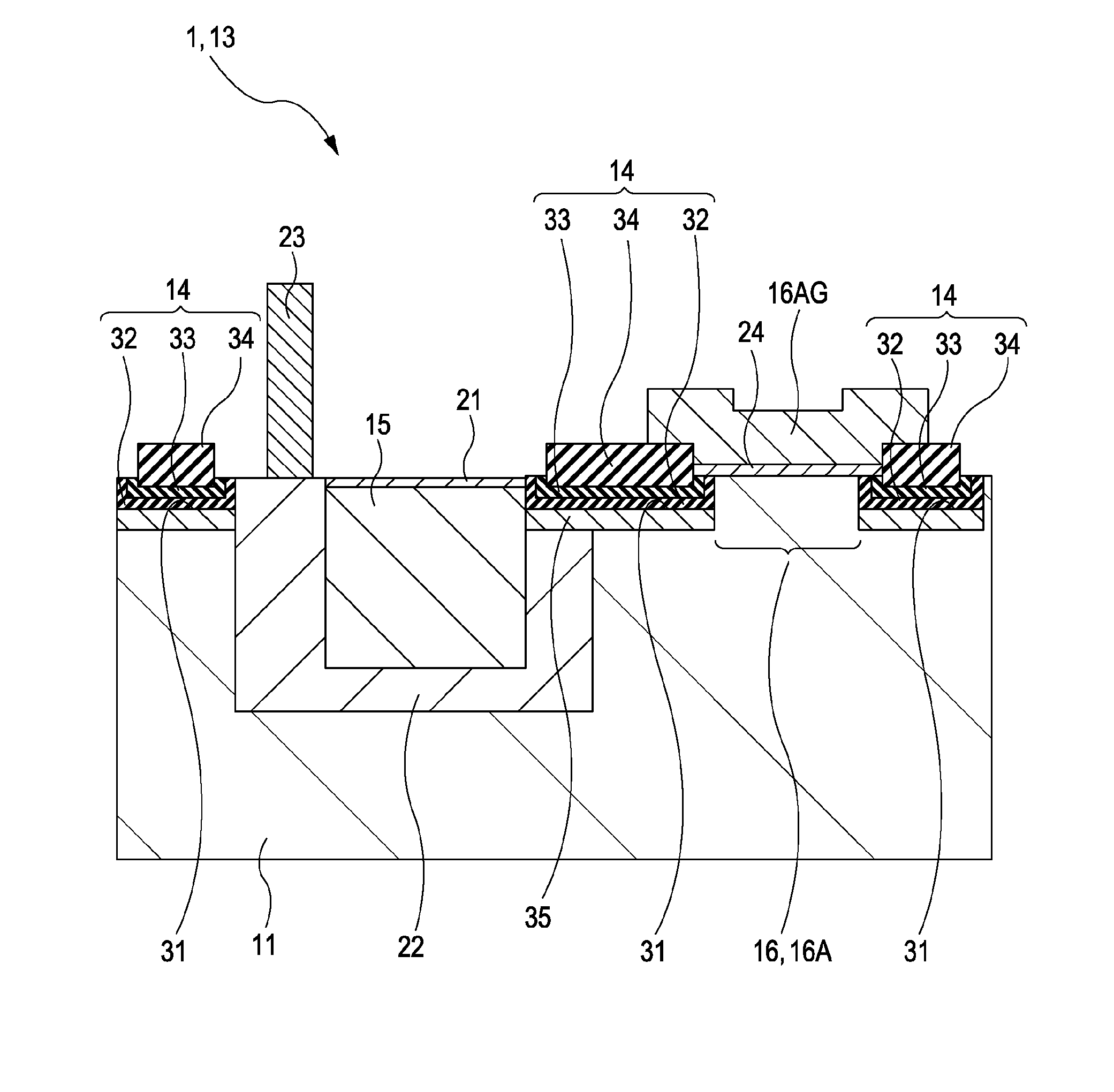
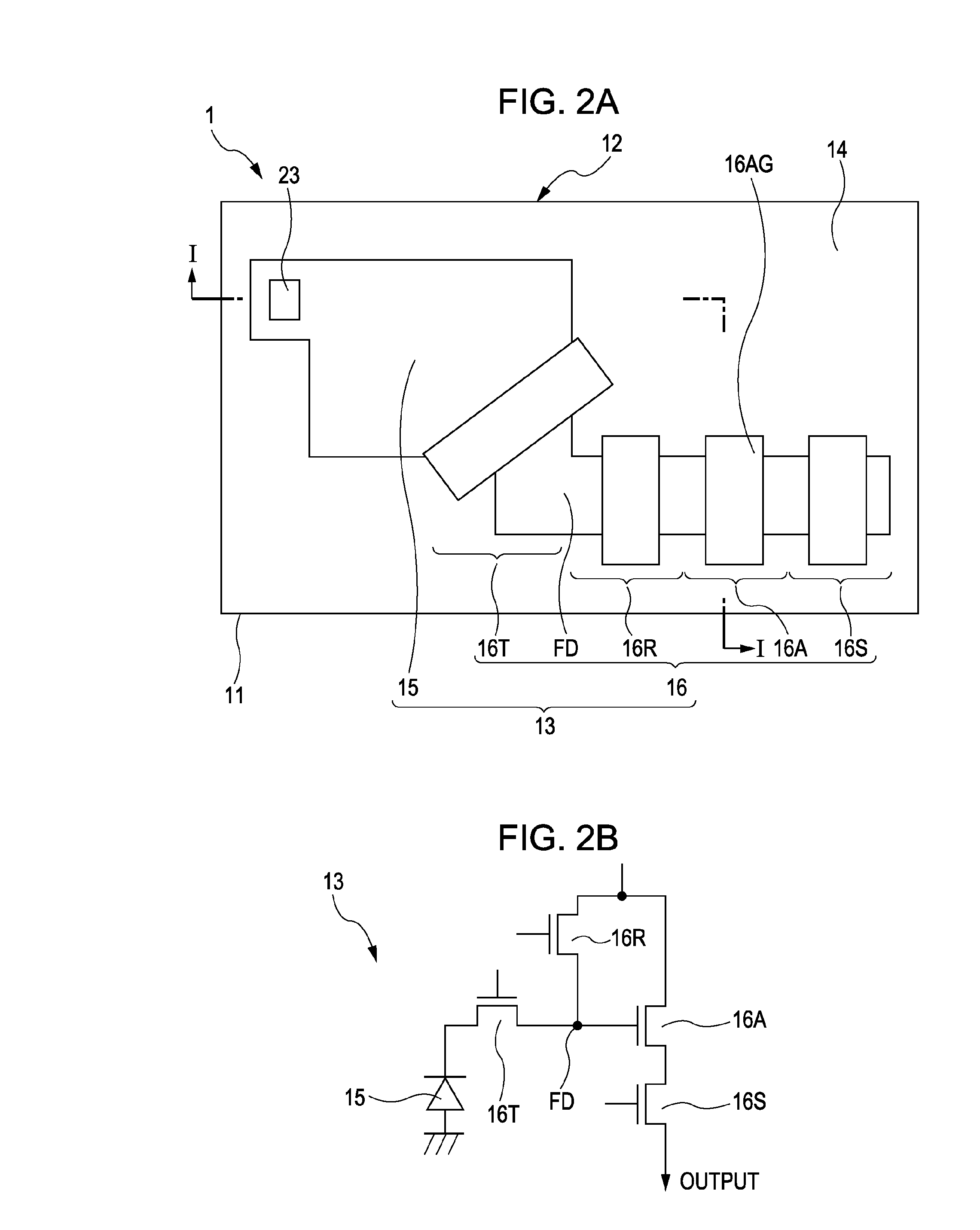
[0041]One example of the configuration of a solid-state imaging device according to a first embodiment of the present invention will be described with reference to a schematic configuration sectional view shown in FIG. 1, a plane layout diagram shown in FIG. 2A, and a circuit diagram shown in FIG. 2B. FIG. 1 is a diagram schematically showing a section taken along a line I-I shown in FIG. 2A.

[0042]As shown in FIGS. 2A and 2B, a solid-state imaging device 1 according to an embodiment of the present invention includes a pixel portion 12, in which a plurality of pixels 13 (one typical pixel is shown in the drawing) are arranged on a semiconductor substrate 11, and a peripheral circuit portion (not shown in the drawing) disposed in the periphery of the pixel portion 12. Furthermore, the above-described pixel portion 12 includes element isolation regions 14 to isolate individual pixels 13. Moreover, the above-described pixel...

second embodiment

[0072]First Example of Method for Manufacturing Solid-State Imaging Device

[0073]A first example of a method for manufacturing a solid-state imaging device, according to a second embodiment of the present invention, will be described with reference to sectional views of production steps shown in FIG. 3A to FIG. 4E.

[0074]As shown in FIG. 3A, a silicon oxide film 71 and a silicon nitride film 72 are formed sequentially on a semiconductor substrate 11. For example, a silicon substrate is used for the above-described semiconductor substrate 11.

[0075]Then, as shown in FIG. 3B, a resist mask (not shown in the drawing) for forming element isolation trenches is formed on the above-described silicon nitride film 72. The resulting mask is used as an etching mask and the above-described silicon nitride film 72, the above-described silicon oxide film 71, and the above-described semiconductor substrate 11 are etched. That is, a first trench 51 for element isolation is formed in a pixel region 17 ...

third embodiment

[0115]Second Example of Method for Manufacturing Solid-State Imaging Device

[0116]A second example of a method for manufacturing a solid-state imaging device, according to a third embodiment of the present invention, will be described with reference to sectional views of production steps shown in FIG. 5A to FIG. 6F.

[0117]As shown in FIG. 5A, a silicon oxide film 71 and a silicon nitride film 72 are formed sequentially on a semiconductor substrate 11. For example, a silicon substrate is used for the above-described semiconductor substrate 11.

[0118]As shown in FIG. 5B, a resist mask (not shown in the drawing) for forming element isolation trenches on the above-described silicon nitride film 72 is formed. The resulting mask is used as an etching mask and the above-described silicon nitride film 72, the above-described silicon oxide film 71, and the above-described semiconductor substrate 11 are etched. That is, a first trench 51 for element isolation is formed in a pixel region 17 of th...


PUM


Abstract

A solid-state imaging device includes, on a semiconductor substrate, a pixel portion having a plurality of pixels provided with a photoelectric conversion portion, which photoelectrically converts incident light to obtain a signal charge and a pixel transistor portion, which converts the signal charge read from the photoelectric conversion portion to a voltage, wherein an element isolation region disposed in the pixel portion includes an insulating film buried in a trench disposed in the semiconductor substrate, and the insulating film includes an insulating film having a negative charge.

Description

BACKGROUND OF THE INVENTION[0001]1. Field of the Invention[0002]The present invention relates to a solid-state imaging device, a method for manufacturing the solid-state imaging device, and an imaging apparatus.[0003]2. Description of the Related Art[0004]In general, shallow trench isolation (STI) is used for element isolation in a finer semiconductor integrated circuit in recent years. However, since STI is provided by digging deeply a trench in a semiconductor substrate, a crystal defect or an interface state occurs at an interface between an insulating film buried in the trench serving for element isolation and the semiconductor substrate so as to become a noise source. Therefore, regarding a CMOS image sensor, in the case where the STI is adopted as a method for element isolation of a pixel portion in parallel with a peripheral circuit, deterioration of a characteristic occurs in such a way that noises are generated at the interface between the semiconductor substrate dug and th...

Claims


Application Information

Patent Timeline
Patent Type & Authority Applications(United States)
IPC IPC(8): H04N5/225H01L31/14H01L31/18H01L27/146
CPCH01L27/14603H01L27/14687H01L27/1463H01L27/14609H01L27/146
Inventor YAMAGUCHI, TETSUJI
Owner SONY CORP
Why Eureka
Try Eureka