Semiconductor optical modulator

a semiconductor and optical modulator technology, applied in the direction of optics, optical waveguide light guides, instruments, etc., can solve the problems of degrading optical modulation characteristics and increasing insertion loss, and achieve the effects of reducing drive voltage, electric field strength, and lengthening interaction length

Inactive Publication Date: 2010-06-10
NEC CORP
View PDF0 Cites 10 Cited by
  • Summary
  • Abstract
  • Description
  • Claims
  • Application Information

AI Technical Summary

Benefits of technology

[0032]The second reason is as follows. It can be expected that after conquering the problem of the above-mentioned velocity mismatch, relaxation of mismatch between the characteristic impedance as a transmission line and an output impedance of a general optical modulator drive circuit can be achieved additionally. Because, since the electromagnetic field distribution of the modulation RF signal tends to distribute widely from around the undoped core layer toward a semiconductor substrate side due to this below cut-off parallel plate structure, the use of a semi-insulating semiconductor as a substrate makes the characteristic impedance that the modulation RF signal senses higher. Therefore, it becomes easy to match it with 50Ω tha

Problems solved by technology

When attaining miniaturization of elements, it becomes a challenge to form bend optical waveguides that connect an optical phase modulator region and an optical multi/demultiplexer smoothly.
There is a fear that such high-order mo

Method used


Image

  • Semiconductor optical modulator
  • Semiconductor optical modulator
  • Semiconductor optical modulator

Examples


first embodiment

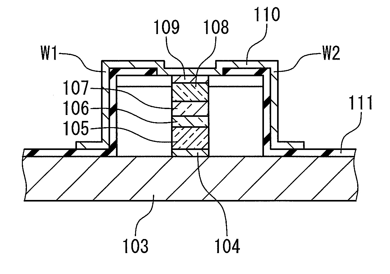
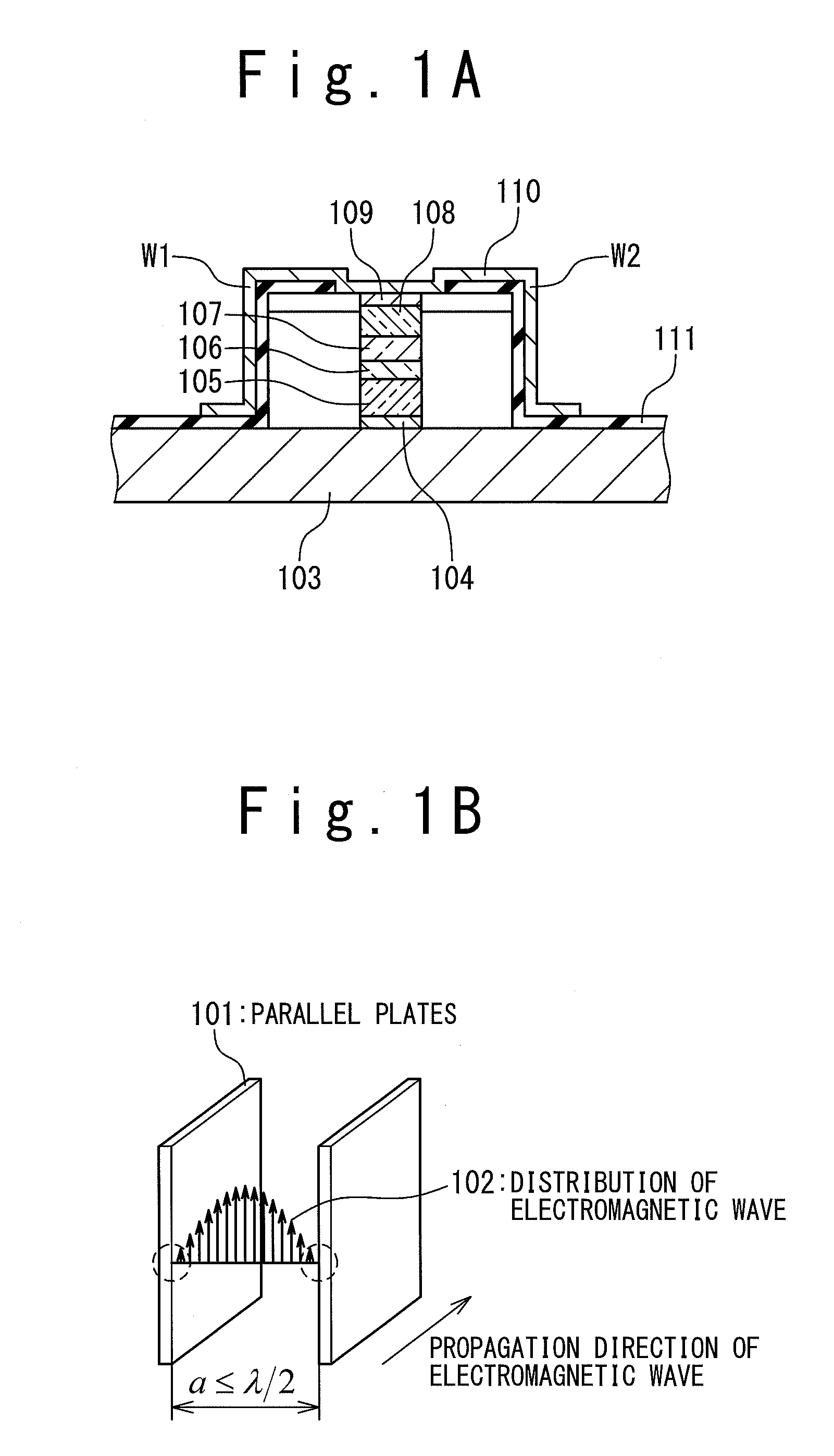
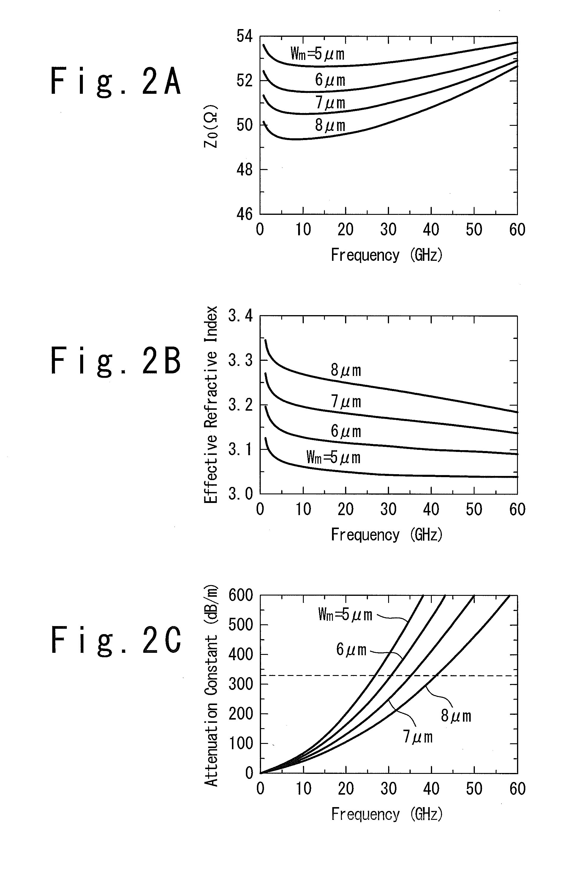
[0071]Hereafter, best mode embodiments for carrying out the present invention will be described in detail referring to drawings. In the present embodiment, a pair of conductor walls almost parallel to the electric field applied to an undoped core layer is provided on both sides of this undoped core layer, and this will functions as below cut-off parallel plates to a modulation RF signal.

[0072]FIG. 1A is a sectional view showing a concrete configuration thereof. The optical modulator in the present embodiment includes a buffer layer 104 formed on a semi-insulating semiconductor substrate 103, a lower clad layer 105 formed on the buffer layer 104, an undoped core layer 106 formed on the lower clad layer 105, an electron injection stop layer 107 formed on the undoped core layer 106, an upper clad layer 108 formed on the electron injection stop layer 107, the upper clad layer 108, and a contact layer 109 formed on the upper clad layer 108. This layered structure forms a stripe shape in ...

second embodiment

[0080]FIG. 4A is a plan view showing a configuration of a semiconductor optical modulator in a second embodiment of the present invention. FIGS. 4B to 4G are sectional views showing a manufacturing process of the semiconductor optical modulator. FIG. 4B shows a cross-sectional structure at the time when the first crystal growth has been completed. FIG. 4C shows a cross-sectional structure at the time when a stripe processing by etching is done. FIG. 4D shows a cross-sectional structure at the time when a process up to buried growth has been completed. FIG. 4E shows a cross-sectional structure at the time when grooves are formed on both sides of an optical waveguide stripe. FIGS. 4F and 4G are diagrams showing cross-sectional structures taken along a line A-A′ and a line B-B′ after electrode formation, respectively. An upper electrode 214 and a lower electrode 215 provide independent electric potentials to the lower clad layer and the upper clad layer, respectively, and constitute a ...

third embodiment

[0090]FIG. 6A is a plan view showing a configuration of a semiconductor Mach Zehnder (MZ) light intensity modulator to which a semiconductor optical modulator in a third embodiment of the present invention is applied. FIGS. 6B to 6G are sectional views showing a manufacturing process of an MZ light intensity modulator. FIG. 6B shows a cross-sectional structure at the time when the process up to the first crystal growth has been completed. FIG. 6C shows a cross-sectional structure at the time when the stripe processing by etching is done. FIG. 6D shows a cross-sectional structure at the time when the process up to a buried growth has been completed. FIG. 6E shows a cross-sectional structure at the time when grooves are formed on both sides of the optical waveguide stripe. FIGS. 6F and 6G show cross-sectional structures taken along a line A-A′ and a line B-B′, respectively, after the electrode formation.

[0091]This element is formed as follows. A buffer layer 402, a lower clad layer 40...


PUM


Abstract

An optical modulator is provided with a stripe-shaped optical waveguide, which has an upper clad layer, a lower clad layer formed between the upper clad layer and a substrate, and an undoped core layer which is arranged between the upper clad layer and the lower clad layer and has a complex refractive index that changes corresponding to the intensity of an applied electric field, to a signal light propagating inside. On the both sides of the stripe-shaped optical waveguide, conductor walls are configured by arranging a pair of parallel blocking flat boards with an insulating wall in between. Thus, the semiconductor optical modulator having a high optical modulation efficiency is provided

Description

TECHNICAL FIELD[0001]The present invention relates to a structure of an optical modulation device. This application is based on Japanese Patent Application No. 2007-61083 that was filed on Mar. 9, 2007. The disclosure of the Japanese Patent Application is hereby incorporated into this application by this reference.BACKGROUND ART[0002]With the explosive increase in demands of broad band multimedia communication services of the Internet, video delivery, etc., introduction of longer-distance, larger-capacity and higher-reliability wavelength division multiplexed optical fiber communication systems is progressing rapidly. In addition, also in subscriber systems, optical fiber access services are rapidly coming into widespread use. In such optical fiber-communication systems, the wavelength multiplexing technique of multiplexing signal lights of a plurality of different wavelengths to transmit is widely employed from a viewpoint of reduction of installation cost of optical fibers that ar...

Claims


Application Information

Patent Timeline
IPC IPC(8): G02F1/03
CPCG02F1/025G02F2201/127G02F2001/0154G02F1/0154
Inventor KATO, TOMOAKI
Owner NEC CORP
Why Eureka
Try Eureka