Method of mask forming and method of three-dimensional microfabrication

a three-dimensional microfabrication and mask technology, applied in the field of three-dimensional microfabrication mask forming and three-dimensional microfabrication, can solve the problems of difficult general definition of blurring, process control and the like, and the limits of high-precision mask formation, etc., to achieve low cost and high accuracy

Inactive Publication Date: 2010-06-10
RIBER
View PDF1 Cites 6 Cited by
  • Summary
  • Abstract
  • Description
  • Claims
  • Application Information

AI Technical Summary

Benefits of technology

[0008]The present invention has been made in view of the circumstances as described above, and an object thereof is to provide a method for forming a mask with a minute width suitable for micr...

Problems solved by technology

However, with regard to optical lithographic techniques by pattern transfer systems, which are currently the mainstream, despite the aim of higher precision by use of extreme ultraviolet radiation or X-rays for example, these have been approaching the limits in terms of high-precision mask formation, photoresist resolution, process control and the like.
According to this meth...

Method used


Image

  • Method of mask forming and method of three-dimensional microfabrication
  • Method of mask forming and method of three-dimensional microfabrication
  • Method of mask forming and method of three-dimensional microfabrication

Examples


first embodiment

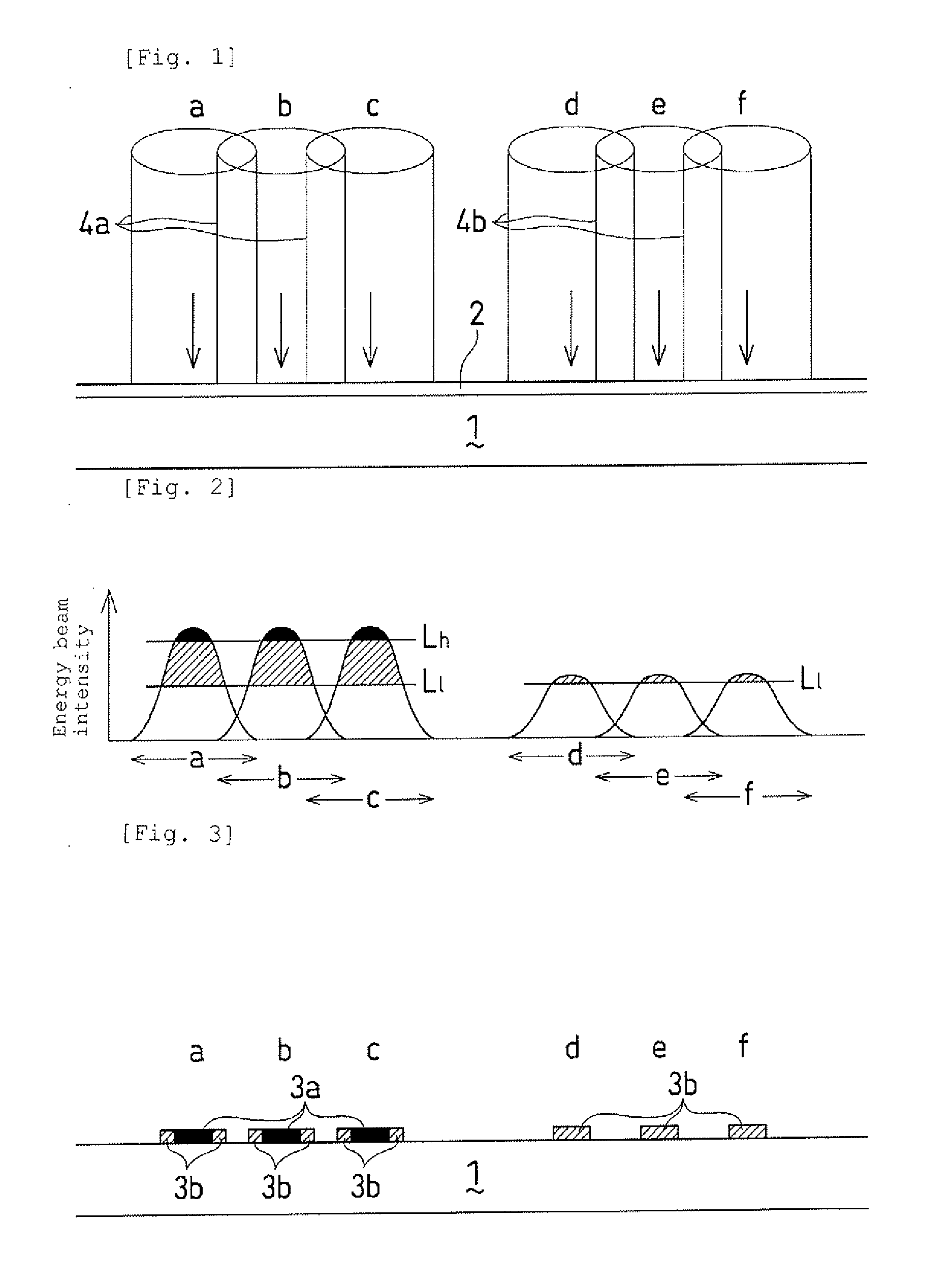
[0054]In a first embodiment, as shown in the left side of FIG. 1, to a GaAs substrate 1, without removing a natural oxide layer 2 of As2O3, As2O, or the like formed naturally on its surface, by means of a publicly-known electron beam drawing device, an electron beam (energy beam) 4a was irradiated in a high vacuum toward the surface of this natural oxide layer 2 (step 1).

[0055]Irradiation of the above-described electron beam 4a was carried out with its beam diameter of 1 μm, an acceleration voltage of 50 kV or less, and the amount of line Dowes of 2.5×10⁻¹ electron / cm, in a single line mode. Here, the amount of line Dowes of the electron beam 4a was controlled by appropriately changing the amperage and irradiation time of the electron beam.

[0056]Here, an irradiation interval of the electron beam 4a (a distance by which, after an electron beam was irradiated, this was translated to a line to be irradiated next) was 50 nm. Namely, the electron beam 4a was irradiated a plurality of tim...

second embodiment

[0074]In this second embodiment, as shown in the right side of FIG. 1, by irradiating an electron beam 4b onto a natural oxide layer 2 of a GaAs substrate 1 and carrying out heating completely the same as the above, a minute mask 3b with a 10 nm width as shown in the right side of FIG. 3 was formed. Here, irradiating conditions of the electron beam 4b were completely the same as those of the foregoing first embodiment expect for that the amount of line Dowes was provided as 2.5×10⁹ electron / cm.

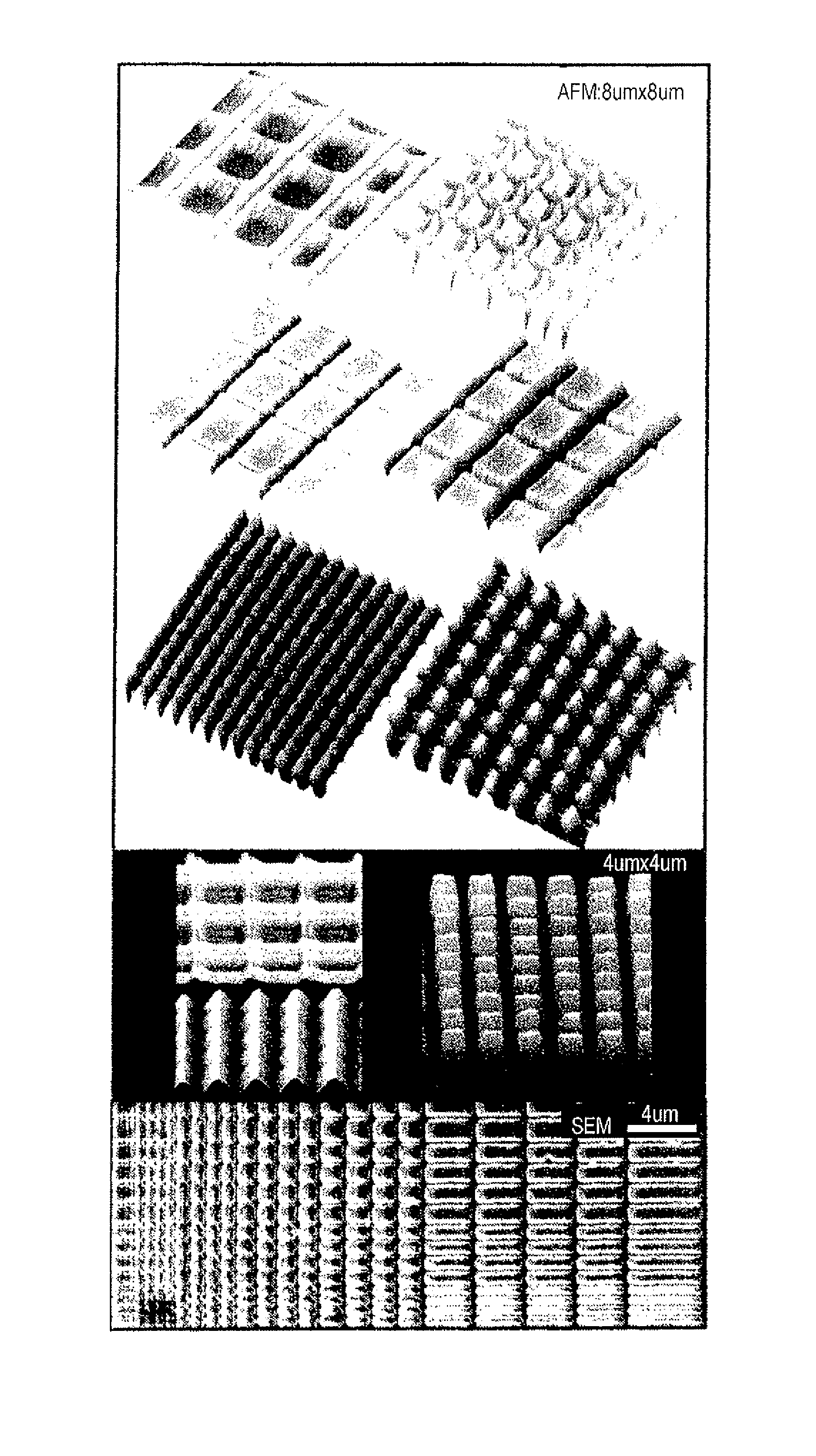
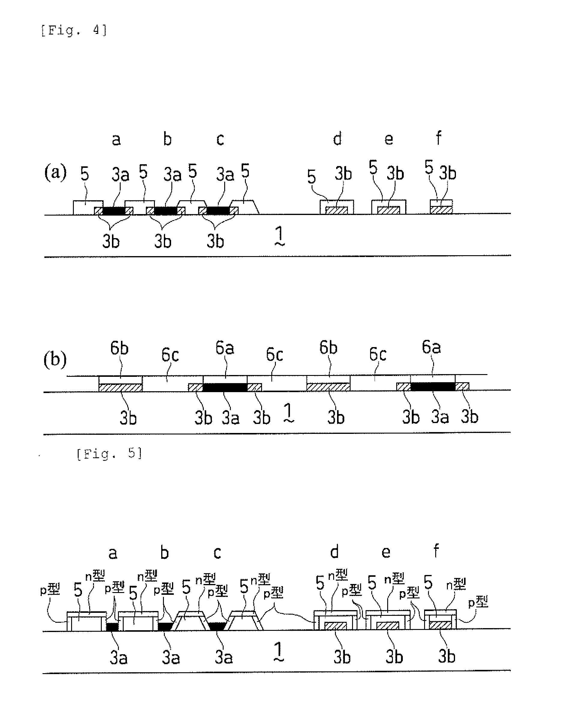
[0075]Then, by an MBE method, GaAs was selectively grown on the GaAs layer 1 of the side where the natural oxide layer 2 had been desorbed. Then, at the initial stage of diffusion, Ga atoms adhered to parts (mask 3b) where Ga2O3 had been formed (unlike the foregoing first embodiment), and by self-assembly around the same as a nucleus, GaAs grown crystals 5 were formed as shown in the right side of FIG. 4(a). Namely, the Ga2O3 (mask 3b) as a reformed natural oxide layer functioned as adsorptive...

third embodiment

[0080]In this third embodiment, onto a GaAs substrate 1, GaAs crystals were grown by self-assembly by means of a technique the same as that of the foregoing first embodiment or second embodiment, a high-density array structure was formed as in FIG. 4(a). Thereafter, Si as being a dopant was supplied as molecular beams. Then, as shown in FIG. 5, an n-channel was formed on a facet surface (crystal orientation (100) surface) of each GaAs grown crystal 5, and p-channels were formed on other facet surfaces (crystal orientation (n11) A surface, n is 3, for example) were formed.

[0081]By this method of the third embodiment, a large number of minute transistor structures could be formed by fewer steps. In other words, p-n control of a surface of each unit structure of a high-density array structure could be carried out in a lump.


PUM


Abstract

The invention provides a method for forming a selective mask on a surface of a layer of AlXGaYIn1-X-YAsZP1-Z or AlXGaYIn1-X-YNZAs1-Z (0≦X≦1, 0≦Y≦1, 0≦Z≦1), which is a method for forming a mask with a minute width suitable for microfabrication in nano-order.
(1) An energy beam 4a, 4b is selectively irradiated onto a natural oxide layer 2 formed on the surface of the layer 1 of AlXGaYIn1-X-YAsZP1-Z or AlXGaYIn1-X-YNZAs1-Z. (2) Of the natural oxide layer 2, parts other than parts onto which the energy beam 4a, 4b has been irradiated is removed by heating. (3) The natural oxide layer 2 of the parts onto which the energy beam 4a, 4b has been irradiated is partially removed by heating while alternatively carrying out a rise and fall in heating temperature.

Description

TECHNICAL FIELD[0001]The present invention relates to a method for forming a selective mask on a surface of a layer of AlXGaYIn1-X-YAsZP1-Z or AlXGaYIn1-X-YNZAs1-Z (0≦X≦1, 0≦Y≦1, 0≦Z≦1), and moreover, to a method for processing a microindentation on the surface of the layer of AlXGaYIn1-X-YAsZP1-Z or AlXGaYIn1-X-YNZAs1-Z.BACKGROUND OF THE INVENTION[0002]For semiconductor microfabrication technologies, currently, 90 nm-level microfabrication has reached the practical stage, however, owing to the rapid sophistication of semiconductor devices in recent years, the importance in development of processing techniques in further microscopic nanoscales has been advocated. Under such circumstances, in Japan, the “Semiconductor MIRAI (Millennium Research for Advanced Information Technology) Project” was started as a national project in fiscal 2001 to work on development and practical use of 45 nm-level microfabrication as a target. In addition, at the private-sector level, the “ASUKA project” ...

Claims


Application Information

Patent Timeline
IPC IPC(8): G03F7/20G03F1/00C23C14/02C23C14/06H01L21/203H01L21/302
CPCB81C1/00428B82Y10/00G03F7/0043H01L21/02395H01L21/02546H01L21/31105H01L21/02639H01L21/02642H01L21/2636H01L21/3086H01L21/02631Y10S430/143Y10S430/146Y10S430/145
Inventor SANO, NAOKATSUKANEKO, TADAAKI
Owner RIBER
Why Eureka
Try Eureka