Method for fabrication of aligned nanowire structures in semiconductor materials for electronic, optoelectronic, photonic and plasmonic devices

a technology of aligned nanowires and semiconductor materials, applied in the direction of semiconductor/solid-state device details, instruments, optical elements, etc., can solve the problems of contaminating grown nanowires and complicating the nanowire fabrication process, so as to improve the spectral brightness, thermal stability and overall efficiency. , the effect of improving the brightness of the beam

Inactive Publication Date: 2010-06-17
ANTEOS INC & ALTAIR CENT
View PDF3 Cites 22 Cited by
  • Summary
  • Abstract
  • Description
  • Claims
  • Application Information

AI Technical Summary

Benefits of technology

[0023]An additional object is to provide method for fabrication of photonic crystal structure and Bragg gratings in active region of p-n junction of laser diodes for improving their spectral brightness, beam quality, thermal stability and overall efficiency.

Problems solved by technology

However, the metal catalysts contaminate the grown nanowires and complicate the nanowire fabrication process.
Therefore, one of the major challenges in fabricating nanowires is to synthesize high purity single-crystalline nanowires without using metals catalysts in the process.

Method used


Image

  • Method for fabrication of aligned nanowire structures in semiconductor materials for electronic, optoelectronic, photonic and plasmonic devices
  • Method for fabrication of aligned nanowire structures in semiconductor materials for electronic, optoelectronic, photonic and plasmonic devices
  • Method for fabrication of aligned nanowire structures in semiconductor materials for electronic, optoelectronic, photonic and plasmonic devices

Examples


Embodiment Construction

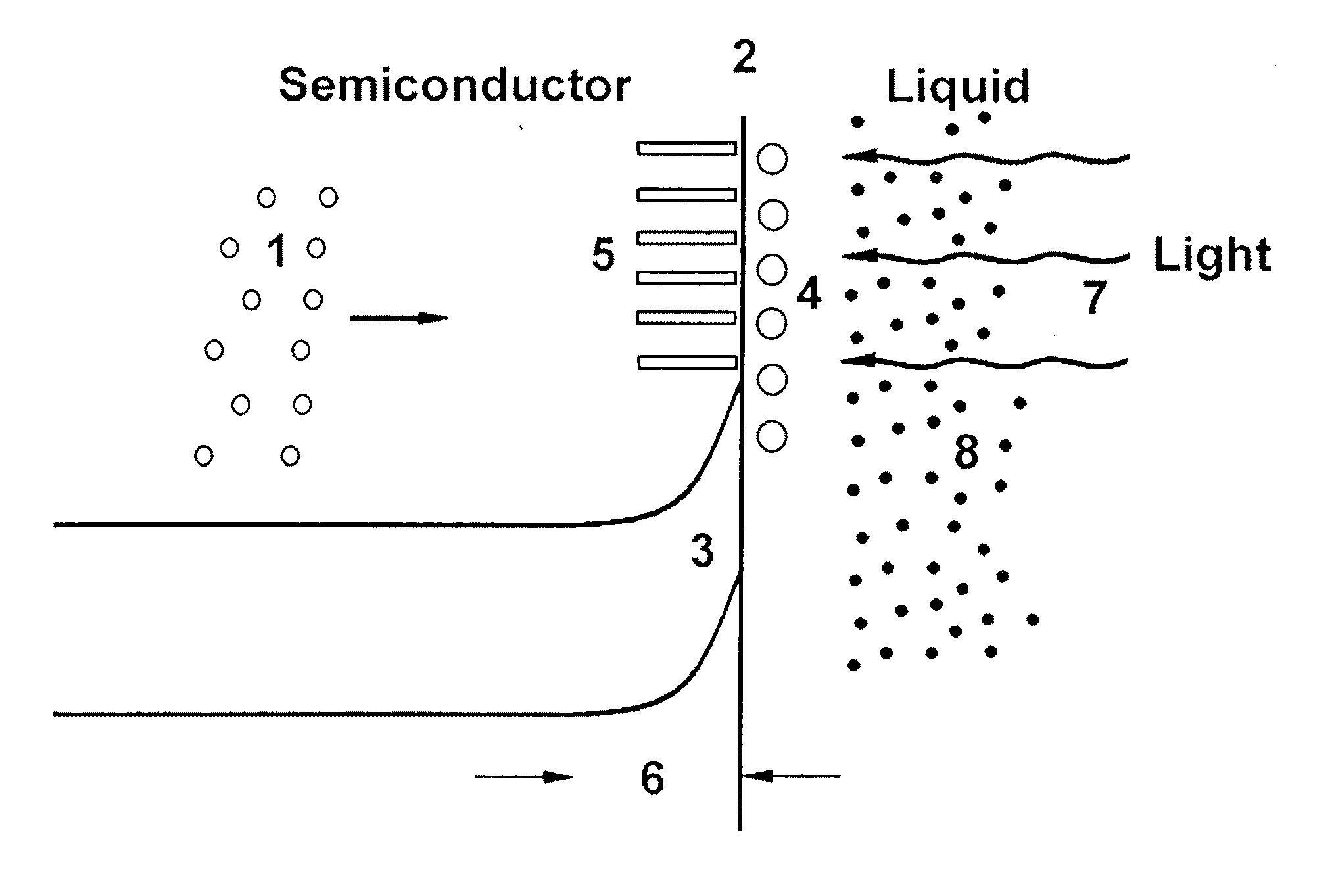
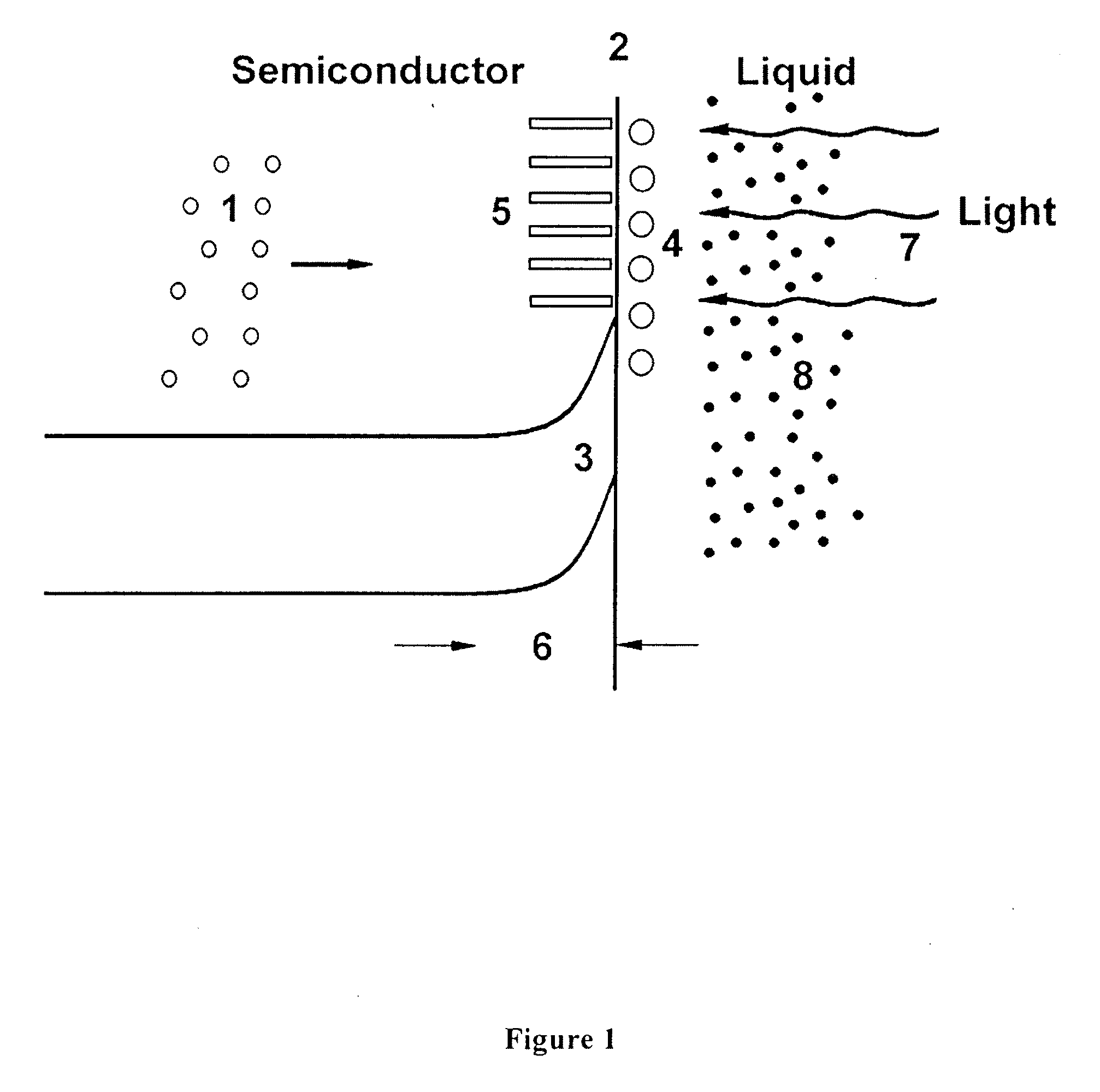
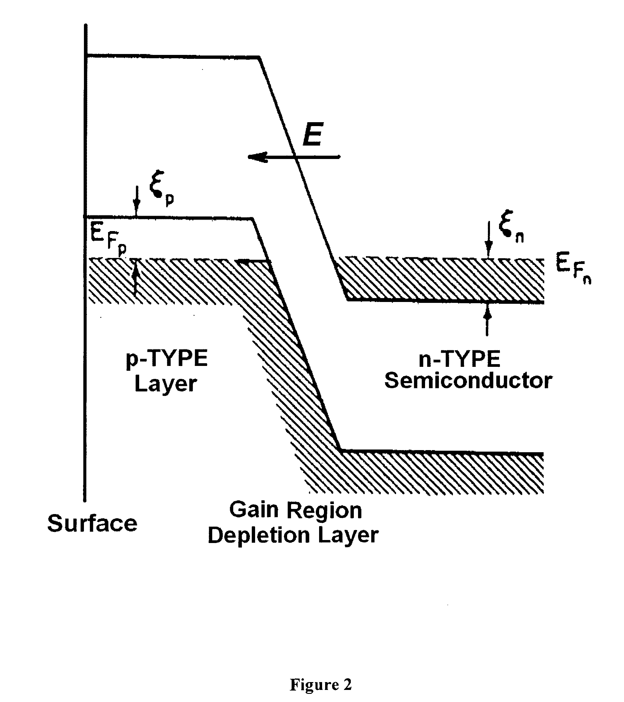
[0045]The preferred embodiments are related to fabrication of the semiconductor nanocomposite materials incorporating aligned metal or semiconductor nanowires using the process of photo-modification of the semiconductor material and application of these semiconductor nanomaterials in electronic, optoelectronic, photonic, and plasmonic devices. The aligned metal or semiconductor nanowires are self-assembled from metal or semiconductor interstitial defect atoms, which are either inherently present in the semiconductor or artificially introduced in the preferred matrix semiconductor material.

[0046]The process of photo-modification can be explained as follows. Any exposed surface of semiconductor has a set of incomplete covalent bonds, which are available for strong interactions with atoms and molecules of the ambient. The density of such bonds at the surface is about 1015 cm−2. The appearing surface states having electron energy levels within the energy bandgap are known as Tamm states...


PUM

PropertyMeasurementUnit
telecommunication wavelengthsaaaaaaaaaa
electron diffusion lengthaaaaaaaaaa

Abstract

The present invention describes a method of fabrication of nanocomposite semiconductor materials comprising aligned arrays of metal or semiconductor nanowires incorporated into semiconductor material for application in various electronic, optoelectronic, photonic and plasmonic devices employing self-assembling of the nanowires under light illumination from charged interstitial defect atoms, which are either inherently present in the semiconductor material or artificially introduced in the matrix semiconductor material.

Description

BACKGROUND OF THE INVENTION[0001]1. Field of the Invention[0002]This invention relates to nanocomposite semiconductor materials and structures for applications in various electronic, optoelectronic, photonic and plasmonic devices, such as inorganic or organic semiconductor materials incorporating aligned nanowires made of metals or semiconductors. It describes a fabrication method employing new process of photo-modification for self-assembling the aligned nanowires and nanowire arrays made of metal or semiconductor materials at specific positions in the near-surface region or in bulk of the matrix semiconductor material, which are defined by light illumination. It also provides examples of some new optoelectronic and photonic components, which could benefit from application of the developed technology and nanocomposite materials. Preferred embodiments include components of diffractive optics, diffraction gratings, phase retardation plates and polarizers operating in both visible and...

Claims


Application Information

Patent Timeline
Patent Type & Authority Applications(United States)
IPC IPC(8): B01J19/12
CPCB82Y20/00B82Y30/00B82Y40/00G02B6/122H01L21/28H01L23/373H01L27/14603H01L2924/0002H01L27/14683H01L29/452H01L31/0264H01L2924/12044H01L2924/00
Inventor KRIVOSHLYKOV, SERGEI
Owner ANTEOS INC & ALTAIR CENT
Why Eureka
Try Eureka